IRLR8726 INFINEON 英飞凌芯片 中文版规格书手册.pdf
需积分: 5 179 浏览量
2023-06-20
11:17:56
上传
评论
收藏 355KB PDF 举报

www.irf.com 1
11/23/09
IRLR8726PbF
IRLU8726PbF
HEXFET
®
Power MOSFET
Notes through are on page 11
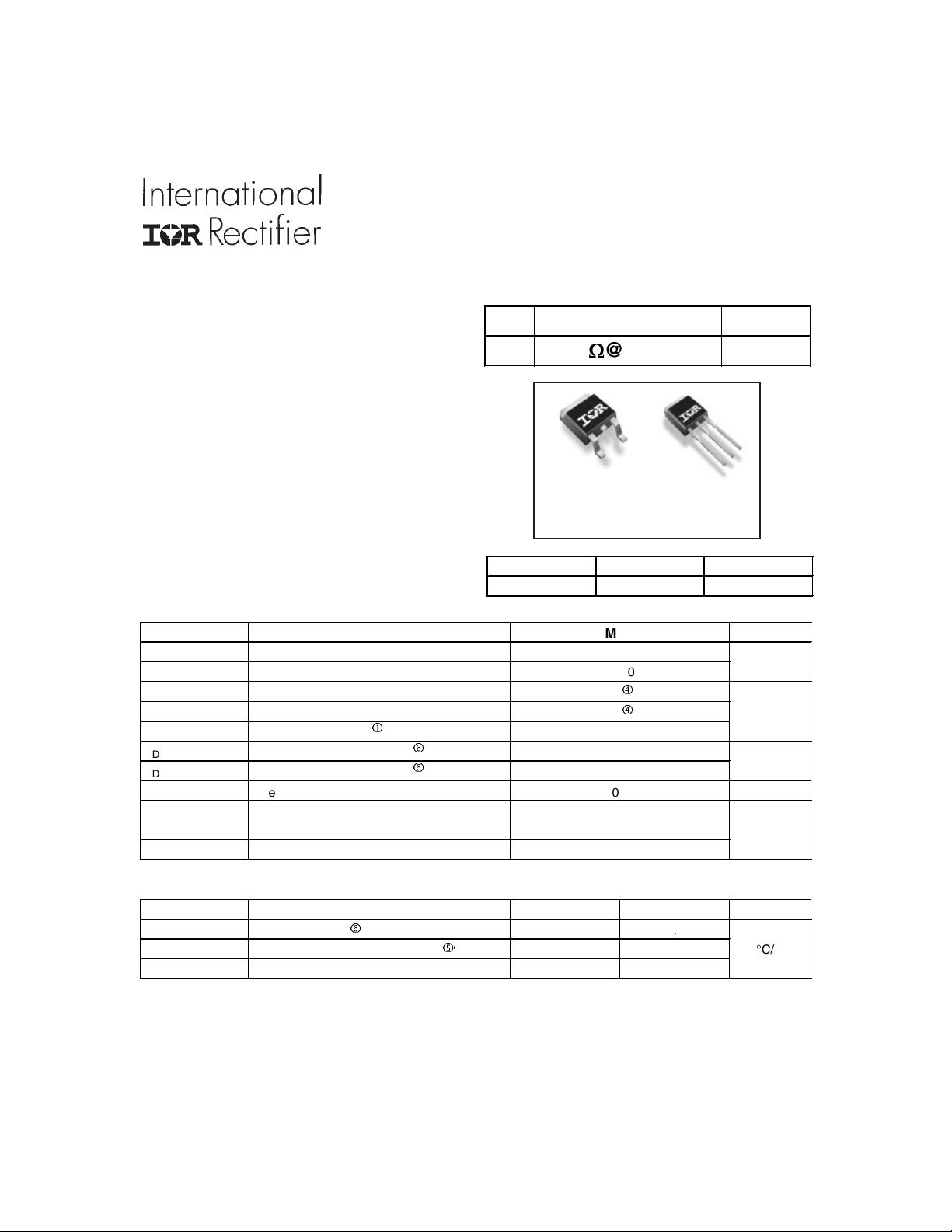
D-Pak
IRLR8726PbF
I-Pak
IRLU8726PbF
S
D
G
S
D
G
GDS
Gate Drain Source
D
D
Benefits
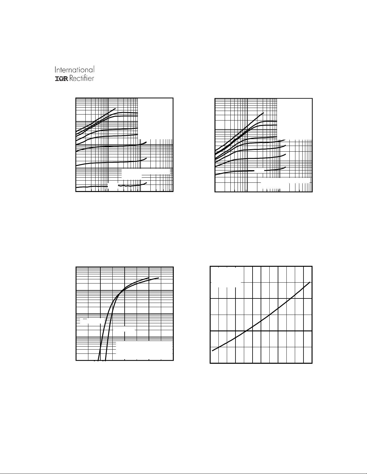
l Very Low R
DS(on)
at 4.5V V
GS
l Ultra-Low Gate Impedance
l Fully Characterized Avalanche Voltage
and Current
l Lead-Free
l RoHS compliant
Applications
l High Frequency Synchronous Buck
Converters for Computer Processor Power
l High Frequency Isolated DC-DC
Converters with Synchronous Rectification
for Telecom and Industrial Use
ORDERING INFORMATION:
See detailed ordering and shipping information on the last page of this data sheet.
V
DSS
R
DS(on)
max
Qg (typ.)
30V
5.8m
:
@V
GS
= 10V
15nC
Absolute Maximum Ratings
Parameter Units
V
DS
Drain-to-Source Voltage V
V
GS
Gate-to-Source Voltage
I
D
@ T
C
= 25°C
Continuous Drain Current, V
GS
@ 10V
I
D
@ T
C
= 100°C
Continuous Drain Current, V
GS
@ 10V
A
I
DM
Pulsed Drain Current
c
P
D
@T
C
= 25°C
Maximum Power Dissipation
h
W
P
D
@T
C
= 100°C
Maximum Power Dissipation
h
Linear Derating Factor W/°C
T
J
Operating Junction and °C
T
STG
Storage Temperature Range
Soldering Temperature, for 10 seconds
Thermal Resistance
Parameter Typ. Max. Units
R
θJC
Junction-to-Case
h
––– 2.0
R
θJA
Junction-to-Ambient (PCB Mount)
gh
––– 50 °C/W
R
θJA
Junction-to-Ambient
h
––– 110
75
Max.
86
f
61
f
340
± 20
30
0.5
38
300 (1.6mm from case)
-55 to + 175
PD - 97146A
剩余10页未读,继续阅读
资源评论


芯脉芯城
- 粉丝: 3
- 资源: 4030


最新资源
- Hive - A Warehousing Solution Over a Map-Reduce.pdf
- 京东商城商品、店铺信息爬虫(基于selenium框架)
- ABB 紧凑型机器人IRB1200-extenal-2017-presentation-0511.pdf
- 基于BP神经网络的风险评估项目 源代码+数据+结论+高分项目.7z
- 云存储实验题目2.docx
- cdr9在win10系统完美解决保存、输出、另存选项遮盖问题drawintl.dll
- 云数据中心运维-大作业.docx
- 基于matlab-simulink 的二级倒立摆设计项目+高分项目.7z
- SpringBoot集成minio实现文件的上传,下载,获取列表,增加桶等的基本操作
- 信号源N5172B使用手册
资源上传下载、课程学习等过程中有任何疑问或建议,欢迎提出宝贵意见哦~我们会及时处理!
点击此处反馈


