没有合适的资源?快使用搜索试试~ 我知道了~
IRLR7843 INFINEON 英飞凌芯片 中文版规格书手册.pdf
需积分: 5 0 下载量 124 浏览量
2023-06-20
11:17:55
上传
评论
收藏 366KB PDF 举报
温馨提示
![preview](https://dl-preview.csdnimg.cn/87932949/0001-0e0da89b45cbf8bc4afbcf622f83237d_thumbnail.jpeg)
![preview-icon](https://csdnimg.cn/release/downloadcmsfe/public/img/scale.ab9e0183.png)
试读
11页
IRLR7843 INFINEON 英飞凌芯片 中文版规格书手册
资源推荐
资源详情
资源评论
![pdf](https://img-home.csdnimg.cn/images/20210720083512.png)
![rar](https://img-home.csdnimg.cn/images/20210720083606.png)
![](https://csdnimg.cn/release/download_crawler_static/87932949/bg1.jpg)
www.irf.com 1
04/30/08
IRLR7843PbF
IRLU7843PbF
HEXFET
®
Power MOSFET
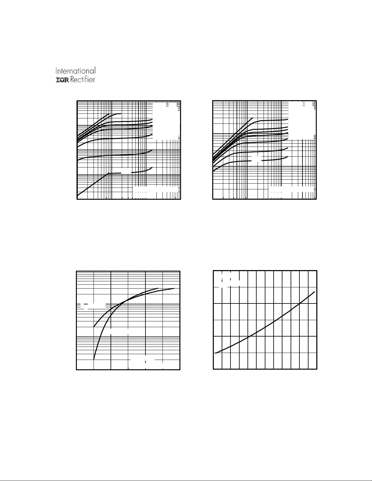
Notes through are on page 11
Applications
Benefits
l Very Low RDS(on) at 4.5V V
GS
l Ultra-Low Gate Impedance
l Fully Characterized Avalanche Voltage
and Current
l High Frequency Synchronous Buck
Converters for Computer Processor Power
l High Frequency Isolated DC-DC
Converters with Synchronous Rectification
for Telecom and Industrial Use
l Lead-Free
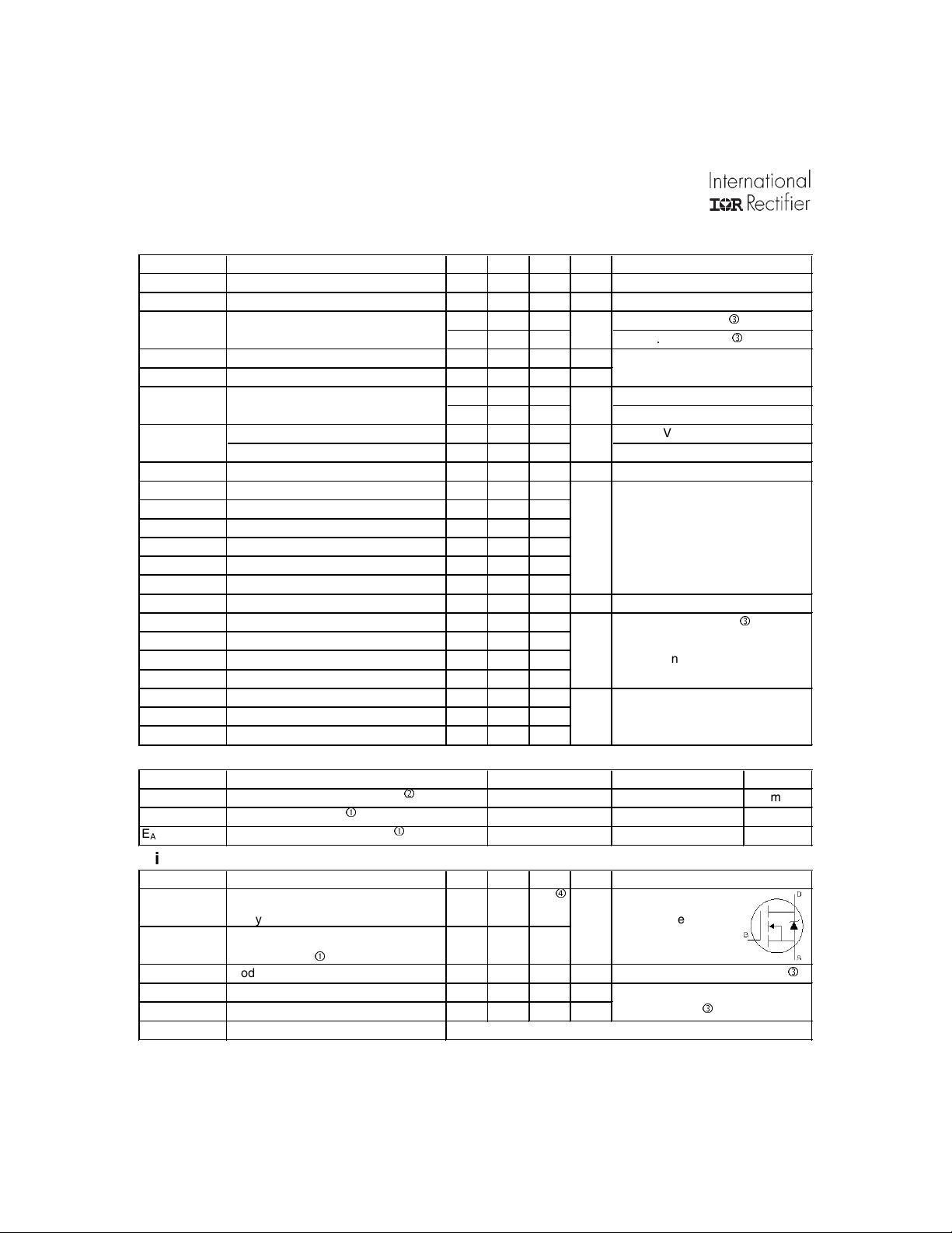
Absolute Maximum Ratings
Parameter Units
V
DS
Drain-to-Source Voltage V
V
GS
Gate-to-Source Voltage
I
D
@ T
C
= 25°C
Continuous Drain Current, V
GS
@ 10V
I
D
@ T
C
= 100°C
Continuous Drain Current, V
GS
@ 10V
A
I
DM
Pulsed Drain Current
c
P
D
@T
C
= 25°C
Maximum Power Dissipation
g
W
P
D
@T
C
= 100°C
Maximum Power Dissipation
g
Linear Derating Factor W/°C
T
J
Operating Junction and °C
T
STG
Storage Temperature Range
Soldering Temperature, for 10 seconds
Thermal Resistance
Parameter Typ. Max. Units
R
θJC
Junction-to-Case ––– 1.05
R
θJA
Junction-to-Ambient (PCB Mount)
g
––– 50 °C/W
R
θJA
Junction-to-Ambient ––– 110
140
Max.
161
f
113
f
620
± 20
30
0.95
71
300 (1.6mm from case)
-55 to + 175
V
DSS
R
DS(on)
max
Qg
30V
3.3m
:
34nC
D-Pak
IRLR7843PbF
I-Pak
IRLU7843PbF
PD - 95440B
![](https://csdnimg.cn/release/download_crawler_static/87932949/bg2.jpg)
IRLR/U7843PbF
2 www.irf.com
Static @ T
J
= 25°C (unless otherwise specified)
Parameter Min. T
y
p. Max. Units
BV
DSS
Drain-to-Source Breakdown Voltage 30 ––– ––– V
∆Β
V
DSS
/
∆
T
J
Breakdown Voltage Temp. Coefficient ––– 19 ––– mV/°C
R
DS(on)
Static Drain-to-Source On-Resistance ––– 2.6 3.3
mΩ
––– 3.2 4.0
V
GS(th)
Gate Threshold Voltage 1.4 ––– 2.3 V
∆
V
GS(th)
/
∆
T
J
Gate Threshold Voltage Coefficient ––– -5.4 ––– mV/°C
I
DSS
Drain-to-Source Leakage Current ––– ––– 1.0 µA
––– ––– 150
I
GSS
Gate-to-Source Forward Leakage ––– ––– 100 nA
Gate-to-Source Reverse Leakage ––– ––– -100
gfs Forward Transconductance 37 ––– ––– S
Q
g
Total Gate Charge ––– 34 50
Q
gs1
Pre-Vth Gate-to-Source Charge ––– 9.1 –––
Q
gs2
Post-Vth Gate-to-Source Charge ––– 2.5 ––– nC
Q
gd
Gate-to-Drain Charge ––– 12 –––
Q
godr
Gate Charge Overdrive ––– 10 ––– See Fig. 16
Q
sw
Switch Char
g
e (Q
gs2
+ Q
gd
)
––– 15 –––
Q
oss
Output Charge ––– 21 ––– nC
t
d(on)
Turn-On Delay Time ––– 25 –––
t
r
Rise Time ––– 42 –––
t
d(off)
Turn-Off Delay Time ––– 34 ––– ns
t
f
Fall Time ––– 19 –––
C
iss
Input Capacitance ––– 4380 –––
C
oss
Output Capacitance ––– 940 ––– pF
C
rss
Reverse Transfer Capacitance ––– 430 –––
Avalanche Characteristics
Parameter Units
E
AS
Si
n
gl
e
P
u
l
se
A
va
l
anc
h
e
E
ner
gy
d
mJ
I
AR
A
va
l
anc
h
e
C
urrent
c
A
E
AR
R
epet
i
t
i
ve
A
va
l
anc
h
e
E
ner
gy
c
mJ
Diode Characteristics
Parameter Min. T
y
p. Max. Units
I
S
Continuous Source Current ––– –––
161
f
(Body Diode) A
I
SM
Pulsed Source Current ––– ––– 620
(
Bod
y
Diode
)
c
V
SD
Diode Forward Voltage ––– ––– 1.0 V
t
rr
Reverse Recovery Time ––– 39 59 ns
Q
rr
Reverse Recovery Charge ––– 36 54 nC
t
on
Forward Turn-On Time
V
DS
= V
GS
, I
D
= 250µA
V
DS
= 24V, V
GS
= 0V
V
DS
= 24V, V
GS
= 0V, T
J
= 125°C
Conditions
14
Max.
1440
12
ƒ = 1.0MHz
I
D
= 12A
V
DS
= 15V
Conditions
V
GS
= 0V, I
D
= 250µA
Reference to 25°C, I
D
= 1mA
V
GS
= 10V, I
D
= 15A
e
V
GS
= 4.5V, I
D
= 12A
e
V
GS
= 20V
V
GS
= -20V
V
DS
= 15V, I
D
= 12A
V
DS
= 15V, V
GS
= 0V
V
DD
= 15V, V
GS
= 4.5V
e
Clamped Inductive Load
T
J
= 25°C, I
F
= 12A, V
DD
= 15V
di/dt = 100A/
µ
s
e
T
J
= 25°C, I
S
= 12A, V
GS
= 0V
e
showing the
integral reverse
p-n junction diode.
Intrinsic turn-on time is negligible (turn-on is dominated by LS+LD)
MOSFET symbol
–––
V
GS
= 4.5V
Typ.
–––
–––
I
D
= 12A
V
GS
= 0V
V
DS
= 15V
![](https://csdnimg.cn/release/download_crawler_static/87932949/bg3.jpg)
IRLR/U7843PbF
www.irf.com 3
Fig 4. Normalized On-Resistance
vs. Temperature
Fig 2. Typical Output CharacteristicsFig 1. Typical Output Characteristics
Fig 3. Typical Transfer Characteristics
2.0 3.0 4.0 5.0
V
GS
, Gate-to-Source Voltage (V)
1
10
100
1000
I
D
,
D
r
a
i
n
-
t
o
-
S
o
u
r
c
e
C
u
r
r
e
n
t
(
Α
)
T
J
= 25°C
T
J
= 175°C
V
DS
= 15V
20µs PULSE WIDTH
-60 -40 -20 0 20 40 60 80 100 120 140 160 180
T
J
, Junction Temperature (°C)
0.5
1.0
1.5
2.0
R
D
S
(
o
n
)
,
D
r
a
i
n
-
t
o
-
S
o
u
r
c
e
O
n
R
e
s
i
s
t
a
n
c
e
(
N
o
r
m
a
l
i
z
e
d
)
I
D
= 30A
V
GS
= 10V
0.1 1 10 100
V
DS
, Drain-to-Source Voltage (V)
0.1
1
10
100
1000
I
D
,
D
r
a
i
n
-
t
o
-
S
o
u
r
c
e
C
u
r
r
e
n
t
(
A
)
2.5V
20µs PULSE WIDTH
Tj = 25°C
VGS
TOP 10V
4.5V
3.7V
3.5V
3.3V
3.0V
2.7V
BOTTOM 2.5V
0.1 1 10 100
V
DS
, Drain-to-Source Voltage (V)
1
10
100
1000
I
D
,
D
r
a
i
n
-
t
o
-
S
o
u
r
c
e
C
u
r
r
e
n
t
(
A
)
2.5V
20µs PULSE WIDTH
Tj = 175°C
VGS
TOP 10V
4.5V
3.7V
3.5V
3.3V
3.0V
2.7V
BOTTOM 2.5V
剩余10页未读,继续阅读
资源评论
![avatar-default](https://csdnimg.cn/release/downloadcmsfe/public/img/lazyLogo2.1882d7f4.png)
![avatar](https://profile-avatar.csdnimg.cn/default.jpg!1)
芯脉芯城
- 粉丝: 3
- 资源: 4031
上传资源 快速赚钱
我的内容管理 展开
我的资源 快来上传第一个资源
我的收益
登录查看自己的收益我的积分 登录查看自己的积分
我的C币 登录后查看C币余额
我的收藏
我的下载
下载帮助
![voice](https://csdnimg.cn/release/downloadcmsfe/public/img/voice.245cc511.png)
![center-task](https://csdnimg.cn/release/downloadcmsfe/public/img/center-task.c2eda91a.png)
安全验证
文档复制为VIP权益,开通VIP直接复制
![dialog-icon](https://csdnimg.cn/release/downloadcmsfe/public/img/green-success.6a4acb44.png)