TI-TRS3318E.pdf
26 浏览量
2023-01-31
13:06:30
上传
评论 4
收藏 945KB PDF 举报


1
2
3
4
5
6
7
8
9
10
20
19
18
17
16
15
14
13
12
11
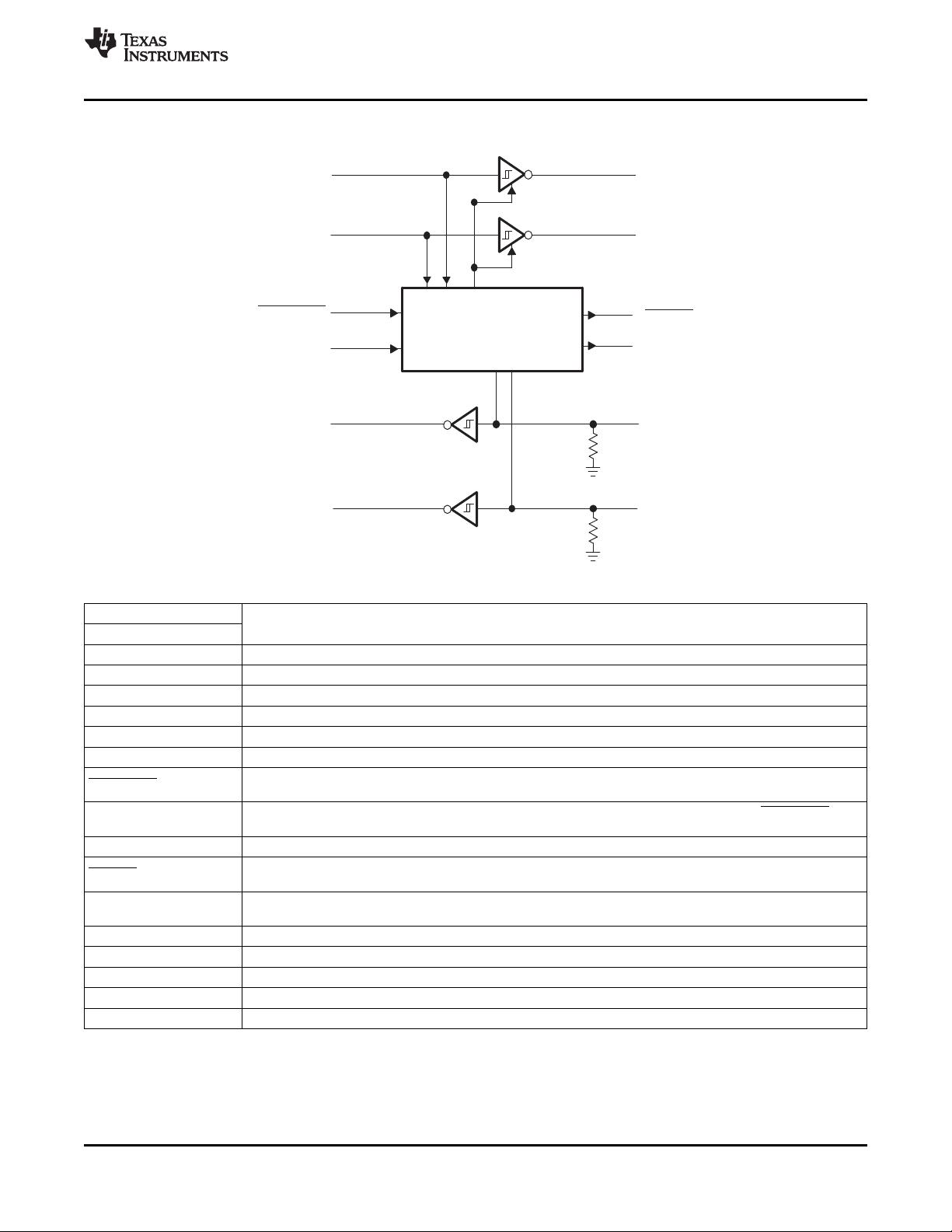
READY
C1+
V+
C1−
C2+
C2−
V−
DOUT2
RIN2
ROUT2
FORCEOFF
V
CC
GND
DOUT1
RIN1
ROUT1
FORCEON
DIN1
DIN2
INVALID
DB OR PW PACKAGE
(TOP VIEW)
TRS3318E
www.ti.com
SLLS805B –APRIL 2007–REVISED OCTOBER 2013
2.5-V 460-kbps RS-232 TRANSCEIVER
WITH ±15-kV ESD PROTECTION
Check for Samples: TRS3318E
1
FEATURES
DESCRIPTION
The TRS3318E is a dual-driver, dual-receiver, RS-
• ESD Protection for RS-232 I/O Pins
232-compatible transceiver. The device features
– ±15 kV (Human-Body Model)
auto-powerdown plus and enhanced electrostatic
– ±8 kV (IEC 61000-4-2, Contact Discharge)
discharge (ESD) protection integrated into the chip.
Driver output and receiver input are protected to ±15
– ±15 kV (IEC 61000-4-2, Air-Gap Discharge)
kV using the IEC 61000-4-2 Air-Gap Discharge
• 300-µA Operating Supply Current
method, ±8 kV using the IEC 61000-4-2 Contact
• 1-µA Low-Power Standby Mode (With
Discharge method, and ±15 kV using the Human-
Receivers Active)
Body Model (HBM).
• Designed to Transmit at a Data Rate of
The device operates at a data rate of 460 kbps. The
460 kbps
transceiver has a proprietary low-dropout driver
output stage, enabling RS-232-compatible operation
• Auto-Powerdown Plus Option Features
from a 2.25-V to 3-V supply with a dual charge pump.
Flexible Power-Saving Mode
The charge pump requires only four 0.1-µF
• Operates From a Single 2.25-V to 3-V V
CC
capacitors and features a logic-level output (READY)
Supply
that asserts when the charge pump is regulating and
• Designed to be Interchangeable With Industry
the device is ready to begin transmitting.
Standard '3318 Devices
The TRS3318E achieves a 1-µA supply current using
the auto-powerdown feature. This device
APPLICATIONS
automatically enters a low-power power-down mode
when the RS-232 cable is disconnected or the drivers
• Battery-Powered Systems
of the connected peripherals are inactive for more
• PDAs
than 30 s. The device turns on again when it senses
• Cellular Phones
a valid transition at any driver or receiver input. Auto-
• Notebooks
powerdown saves power without changes to the
existing BIOS or operating system.
• Hand-Held Equipment
This device is available in two space-saving
• Pagers
packages: 20-pin SSOP and 20-pin TSSOP.
1
Please be aware that an important notice concerning availability, standard warranty, and use in critical applications of
Texas Instruments semiconductor products and disclaimers thereto appears at the end of this data sheet.
PRODUCTION DATA information is current as of publication date.
Copyright © 2007–2013, Texas Instruments Incorporated
Products conform to specifications per the terms of the Texas
Instruments standard warranty. Production processing does not
necessarily include testing of all parameters.


剩余21页未读,继续阅读
资源评论


