DS125BR800A
SNLS467 –NOVEMBER 2013
www.ti.com
Table 1. Pin Descriptions
(1)
Pin Name Pin Number I/O, Type Pin Description
Differential High Speed I/O's
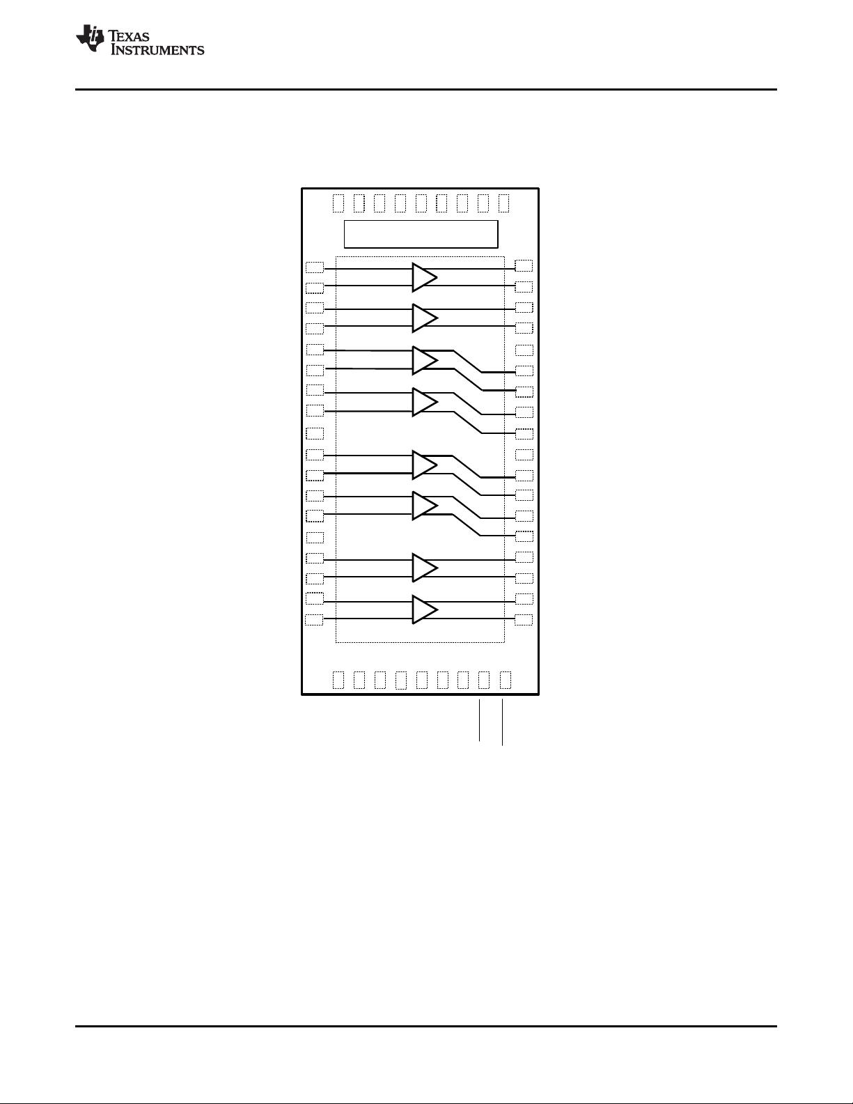
INB_0+, INB_0-,INB_1+, 1, 2, 3, 4, I Inverting and non-inverting CML differential inputs to the equalizer. On-
INB_1-,INB_2+, INB_2- 5, 6, 7, 8, chip 50Ω termination resistor connects INB_n+ to VDD and INB_n- to
,INB_3+, INB_3- VDD when enabled.
AC coupling required on high-speed I/O
INA_0+, INA_0-,INA_1+, 10, 11, 12, 13, I Inverting and non-inverting CML differential inputs to the equalizer. On-
INA_1-,INA_2+, INA_2- 15, 16, 17, 18 chip 50Ω termination resistor connects INA_n+ to VDD and INA_n- to
,INA_3+, INA_3- VDD when enabled.
AC coupling required on high-speed I/O
OUTB_0+, OUTB_0-, 45, 44, 43, 42, O Inverting and non-inverting 50Ω driver outputs with de-emphasis.
OUTB_1+, OUTB_1-, 40, 39, 38, 37 Compatible with AC coupled CML inputs.
OUTB_2+, OUTB_2-, AC coupling required on high-speed I/O
OUTB_3+, OUTB_3-
OUTA_0+, OUTA_0-, 35, 34, 33, 32, O Inverting and non-inverting 50Ω driver outputs with de-emphasis.
OUTA_1+, OUTA_1-, 31, 30, 29, 28 Compatible with AC coupled CML inputs.
OUTA_2+, OUTA_2-, AC coupling required on high-speed I/O
OUTA_3+, OUTA_3-
Control Pins — Shared (LVCMOS)
ENSMB 48 I, 4-LEVEL System Management Bus (SMBus) enable pin
Tie 1kΩ to VDD = Register Access SMBus Slave Mode
FLOAT = Read External EEPROM (Master SMBUS Mode)
Tie 1kΩ to GND = Pin Mode
ENSMB = 1 (SMBUS MODE)
SCL 50 I, LVCMOS ENSMB Master or Slave mode
O, OPEN Drain SMBUS clock input is enabled (slave mode).
Clock output when loading EEPROM configuration (master mode).
SDA 49 I, LVCMOS, ENSMB Master or Slave mode
O, OPEN Drain The SMBus bidirectional SDA pin is enabled. Data input or open drain
(pull-down only) output.
AD0-AD3 54, 53, 47, 46 I, LVCMOS ENSMB Master or Slave mode
SMBus Slave Address Inputs. In SMBus mode, these pins are the user
set SMBus slave address inputs.
READ_EN 26 I, LVCMOS When using an External EEPROM, a transition from high to low starts
the load from the external EEPROM
ENSMB = 0 (PIN MODE)
EQA0, EQA1, 20, 19, I, 4-LEVEL EQA[1:0] and EQB[1:0] control the level of equalization on the input pins.
EQB0, EQB1 46, 47 The pins are active only when ENSMB is de-asserted (low). The 8
channels are organized into two banks. Bank A is controlled with the
EQA[1:0] pins and bank B is controlled with the EQB[1:0] pins. When
ENSMB goes high the SMBus registers provide independent control of
each channel. The EQB[1:0] pins are converted to SMBUS AD2/AD3
inputs. See Table 3.
DEMA0, DEMA1, 49, 50, I, 4-LEVEL DEMA[1:0] and DEMB[1:0] control the level of de-emphasis of the output
DEMB0, DEMB1 53, 54 driver. The pins are only active when ENSMB is de-asserted (low). The 8
channels are organized into two banks. Bank A is controlled with the
DEMA[1:0] pins and bank B is controlled with the DEMB[1:0] pins. When
ENSMB goes high the SMBus registers provide independent control of
each channel. The DEMA[1:0] pins are converted to SMBUS SCL/SDA
and DEMB[1:0] pins are converted to AD0, AD1 inputs.
See Table 4.
MODE 21 I, 4-LEVEL MODE control pin selects operating modes.
Tie 1kΩ to GND = GEN 1,2 and SAS/SATA (up to 6 Gbps)
FLOAT = AUTO Rate Select (for PCIe)
Tie 20kΩ to GND = SAS-3 and GEN-3 without De-emphasis
Tie 1kΩ to VDD = SAS-3 and GEN-3 with De-emphasis
See Table 7
(1) LVCMOS inputs without the "FLOAT" conditions must be driven to a logic low or high at all times or operation is not guaranteed.
Input edge rate for LVCMOS/FLOAT inputs must be faster than 50 ns from 10–90%.
For 3.3V mode operation, VIN pin = 3.3V and the "VDD" for the 4-level input is 3.3V.
For 2.5V mode operation, VDD pin = 2.5V and the "VDD" for the 4-level input is 2.5V.
4 Submit Documentation Feedback Copyright © 2013 , Texas Instruments Incorporated
Product Folder Links: DS125BR800A


 我的内容管理
展开
 我的资源
快来上传第一个资源
 我的收益 登录查看自己的收益
 我的积分
登录查看自己的积分
 我的C币
登录后查看C币余额
 我的收藏
我的收藏  我的下载
我的下载  下载帮助
下载帮助 
 前往需求广场,查看用户热搜

 信息提交成功