没有合适的资源?快使用搜索试试~ 我知道了~
TI-CC1021.pdf
需积分: 9 0 下载量 53 浏览量
2022-12-16
21:18:12
上传
评论 4
收藏 2.26MB PDF 举报
温馨提示
试读
90页
TI-CC1021.pdf
资源推荐
资源详情
资源评论
Product
Folder
Order
Now
Technical
Documents
Tools &
Software
Support &
Community
An IMPORTANT NOTICE at the end of this data sheet addresses availability, warranty, changes, use in safety-critical applications,
intellectual property matters and other important disclaimers. PRODUCTION DATA.
CC1021
SWRS045F –JANUARY 2006–REVISED NOVEMBER 2018
CC1021 Single-Chip Low-Power RF Transceiver for Narrowband Systems
Not Recommended for New Designs NRND
1 Device Overview
1
1.1 Features
1
• True Single-Chip UHF RF Transceiver
• Frequency Range 402 MHz to 470 MHz and
804 MHz to 930 MHz
• High Sensitivity
– Up to –112 dBm for 38.4 kHz Receiver Channel
Filter Bandwidth
– Up to –106 dBm for 102.4 kHz Receiver
Channel Filter Bandwidth
• Programmable Output Power
• Low Current Consumption
– RX: 19.9 mA
• Low Supply Voltage
– From 2.3 V to 3.6 V
• Very Few External Components Required
• Small Size
– QFN 32 Package
• Pb-Free Package
• Digital RSSI and Carrier Sense Indicator
• Data Rate Up to 153.6 kBaud
• OOK, FSK, and GFSK Data Modulation
• Integrated Bit Synchronizer
• Image Rejection Mixer
• Programmable Frequency
• Automatic Frequency Control (AFC)
• Suitable for Frequency Hopping Systems
• Suited for Systems Targeting Compliance With
EN 300 220 and FCC CFR47 Part 15
• Easy-to-Use Software for Generating the CC1021
Configuration Data
• Fully Compatible With CC1020 for Receiver
Channel Filter Bandwidths of 38.4 kHz and Higher
1.2 Applications
• Low-Power UHF Wireless Data Transmitters and
Receivers With Channel Spacings
of 50 kHz or Higher
• 433-, 868-, 915-, 930-MHz ISM/SRD Band
Systems
• AMR – Automatic Meter Reading
• Wireless Alarm and Security Systems
• Home Automation
• Low-Power Telemetry
• Automotive (RKE/TPMS)
1.3 Description
The CC1021 device is a true single-chip UHF transceiver designed for very low power and very low
voltage wireless applications. The circuit is mainly intended for the ISM (Industrial, Scientific and Medical)
and SRD (Short Range Device) frequency bands at 433 MHz, 868 MHz, and 915 MHz, but can easily be
programmed for multichannel operation at other frequencies in the 402- to 470-MHz and 804- to 930-MHz
range.
The CC1021 device is especially suited for narrowband systems with channel spacing of 50 kHz and
higher complying with EN 300 220 and CC CFR47 part 15.
The CC1021 device main operating parameters can be programmed through a serial bus, thus making the
CC1021 device a very flexible and easy to use transceiver.
In a typical system, the CC1021 device is used together with a microcontroller and a few external passive
components.
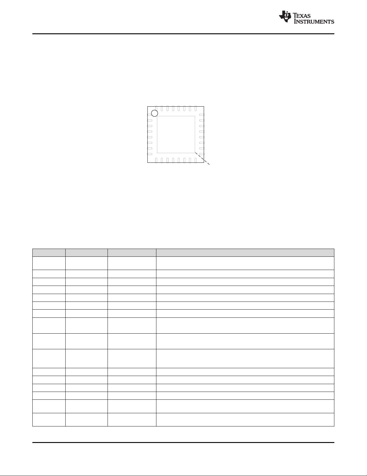
(1) For more information, see Section 8, Mechanical Packaging and Orderable Information.
Table 1-1. Device Information
(1)
PART NUMBER PACKAGE BODY SIZE (NOM)
CC1021 VQFNP (32) 7.00 mm × 7.00 mm
DIO
LOCK
DCLK
RF_IN
LNA
FREQ
SYNTH
DIGITAL
DEMODULATOR
- Digital RSSI
- Gain Control
- Image Suppression
- Channel Filtering
- Demodulation
DIGITAL
MODULATOR
- Modulation
- Data shaping
- Power Control
BIAS
Power
Control
DIGITAL
INTERFACE
TO mC
CONTROL
LOGIC
PA
ADC
ADC
RF_OUT
R_BIAS
XOSC_Q1 XOSC_Q2
PDO
XOSC
VC
CHP_OUT
LNA 2
0
90
:2
0
90
:2
Multiplexer
Multiplexer
PA_EN
LNA_EN
PCLK
PDI
PSEL
Not Recommended for New Designs NRND
2
CC1021
SWRS045F –JANUARY 2006–REVISED NOVEMBER 2018
www.ti.com
Submit Documentation Feedback
Product Folder Links: CC1021
Device Overview Copyright © 2006–2018, Texas Instruments Incorporated
1.4 Functional Block Diagram
Figure 1-1 shows the system block diagram of the CC1021 device.
Figure 1-1. Functional Block Diagram
Not Recommended for New Designs NRND
3
CC1021
www.ti.com
SWRS045F –JANUARY 2006–REVISED NOVEMBER 2018
Submit Documentation Feedback
Product Folder Links: CC1021
Revision HistoryCopyright © 2006–2018, Texas Instruments Incorporated
Table of Contents
1 Device Overview ......................................... 1
1.1 Features .............................................. 1
1.2 Applications........................................... 1
1.3 Description............................................ 1
1.4 Functional Block Diagram ............................ 2
2 Revision History ......................................... 3
3 Terminal Configuration and Functions.............. 4
3.1 Pin Diagram .......................................... 4
3.2 Pin Configuration ..................................... 4
4 Specifications ............................................ 6
4.1 Absolute Maximum Ratings .......................... 6
4.2 ESD Ratings.......................................... 6
4.3 Recommended Operating Conditions ................ 6
4.4 RF Transmit .......................................... 6
4.5 RF Receive ........................................... 8
4.6 RSSI / Carrier Sense................................ 10
4.7 Intermediate Frequency (IF) ........................ 11
4.8 Crystal Oscillator .................................... 11
4.9 Frequency Synthesizer.............................. 12
4.10 Digital Inputs / Outputs.............................. 12
4.11 Current Consumption ............................... 13
4.12 Thermal Resistance Characteristics for VQFNP
Package ............................................. 14
5 Detailed Description ................................... 15
5.1 Overview ............................................ 15
5.2 Functional Block Diagram........................... 15
5.3 Configuration Overview ............................. 16
5.4 Microcontroller Interface............................. 17
5.5 4-wire Serial Configuration Interface................ 18
5.6 Signal Interface...................................... 20
5.7 Data Rate Programming ............................ 22
5.8 Frequency Programming ............................ 24
5.9 Receiver............................................. 25
5.10 Transmitter .......................................... 38
5.11 Input and Output Matching and Filtering............ 40
5.12 Frequency Synthesizer.............................. 44
5.13 VCO and LNA Current Control...................... 48
5.14 Power Management................................. 48
5.15 On-Off Keying (OOK) ............................... 50
5.16 Crystal Oscillator .................................... 51
5.17 Built-in Test Pattern Generator ..................... 53
5.18 Interrupt on Pin DCLK............................... 54
5.19 PA_EN and LNA_EN Digital Output Pins ........... 54
5.20 System Considerations and Guidelines ............. 55
5.21 Antenna Considerations............................. 58
5.22 Configuration Registers ............................. 59
6 Applications, Implementation, and Layout........ 78
6.1 Application Information .............................. 78
6.2 Design Requirements ............................... 80
6.3 PCB Layout Guidelines ............................. 81
7 Device and Documentation Support ............... 82
7.1 Device Support ...................................... 82
7.2 Documentation Support ............................. 82
7.3 Trademarks.......................................... 83
7.4 Electrostatic Discharge Caution..................... 83
7.5 Export Control Notice ............................... 83
7.6 Glossary............................................. 83
8 Mechanical Packaging and Orderable
Information .............................................. 83
8.1 Packaging Information .............................. 83
2 Revision History
Changes from August 20, 2016 to November 30, 2018 Page
• Global: Changed upper frequency from 960 MHz to 930 MHz ................................................................. 1
• Global: Removed references to ARIB STD-T96 .................................................................................. 1
PCLK
1
VC
24
AVDD
23
AVDD
22
RF_OUT
21
AVDD
20
RF_IN
19
AVDD
18
R_BIAS
17
AVDD
16
PA_EN
15
LNA_EN
14
AVDD
13
AVDD
12
XOSC_Q2
11
XOSC_Q1
10
LOCK
9
DIO
8
DCLK
7
DGND
6
DVDD
5
DGND
4
PDO
3
PDI
2
32
PSEL
31
DVDD
30
DGND
29
AVDD
28
CHP_OUT
27
AVDD
26
AD_REF
25
AGND
AGND
Exposed die
attached pad
Not Recommended for New Designs NRND
4
CC1021
SWRS045F –JANUARY 2006–REVISED NOVEMBER 2018
www.ti.com
Submit Documentation Feedback
Product Folder Links: CC1021
Terminal Configuration and Functions Copyright © 2006–2018, Texas Instruments Incorporated
(1) DCLK, DIO and LOCK are high-impedance (3-state) in power down (BIAS_PD = 1 in the MAIN register).
(2) The exposed die attached pad must be soldered to a solid ground plane as this is the main ground connection for the chip.
3 Terminal Configuration and Functions
3.1 Pin Diagram
Figure 3-1 shows pin names and locations for the CC1021 device.
Figure 3-1. Package 7-mm × 7-mm VQFNP (Top View)
3.2 Pin Configuration
Table 3-1. Pin Attributes
(1)(2)
PIN NO. PIN NAME TYPE DESCRIPTION
— AGND Ground (analog)
Exposed die attached pad. Must be soldered to a solid ground plane as this is the
ground connection for all analog modules. See Section 6.3 for more details.
1 PCLK Digital input Programming clock for SPI configuration interface
2 PDI Digital input Programming data input for SPI configuration interface
3 PDO Digital output Programming data output for SPI configuration interface
4 DGND Ground (digital) Ground connection (0 V) for digital modules and digital I/O
5 DVDD Power (digital) Power supply (3 V typical) for digital modules and digital I/O
6 DGND Ground (digital) Ground connection (0 V) for digital modules (substrate)
7 DCLK Digital output
Clock for data in both receive and transmit mode
Can be used as receive data output in asynchronous mode
8 DIO Digital input/output
Data input in transmit mode; data output in receive mode
Can also be used to start power-up sequencing in receive
9 LOCK Digital output
PLL Lock indicator, active low. Output is asserted (low) when PLL is in lock. The
pin can also be used as a general digital output, or as receive data output in
synchronous NRZ/Manchester mode
10 XOSC_Q1 Analog input Crystal oscillator or external clock input
11 XOSC_Q2 Analog output Crystal oscillator
12 AVDD Power (analog) Power supply (3 V typical) for crystal oscillator
13 AVDD Power (analog) Power supply (3 V typical) for the IF VGA
14 LNA_EN Digital output
General digital output. Can be used for controlling an external LNA if higher
sensitivity is needed.
15 PA_EN Digital output
General digital output. Can be used for controlling an external PA if higher output
power is needed.
Not Recommended for New Designs NRND
5
CC1021
www.ti.com
SWRS045F –JANUARY 2006–REVISED NOVEMBER 2018
Submit Documentation Feedback
Product Folder Links: CC1021
Terminal Configuration and FunctionsCopyright © 2006–2018, Texas Instruments Incorporated
Table 3-1. Pin Attributes
(1)(2)
(continued)
PIN NO. PIN NAME TYPE DESCRIPTION
16 AVDD Power (analog) Power supply (3 V typical) for global bias generator and IF anti-alias filter
17 R_BIAS Analog output Connection for external precision bias resistor (82 kΩ, ±1%)
18 AVDD Power (analog) Power supply (3 V typical) for LNA input stage
19 RF_IN RF Input RF signal input from antenna (external AC-coupling)
20 AVDD Power (analog) Power supply (3 V typical) for LNA
21 RF_OUT RF output RF signal output to antenna
22 AVDD Power (analog) Power supply (3 V typical) for LO buffers, mixers, prescaler, and first PA stage
23 AVDD Power (analog) Power supply (3 V typical) for VCO
24 VC Analog input VCO control voltage input from external loop filter
25 AGND Ground (analog) Ground connection (0 V) for analog modules (guard)
26 AD_REF Power (analog) 3 V reference input for ADC
27 AVDD Power (analog) Power supply (3 V typical) for charge pump and phase detector
28 CHP_OUT Analog output PLL charge pump output to external loop filter
29 AVDD Power (analog) Power supply (3 V typical) for ADC
30 DGND Ground (digital) Ground connection (0 V) for digital modules (guard)
31 DVDD Power (digital) Power supply connection (3 V typical) for digital modules
32 PSEL Digital input
Programming chip select, active low, for configuration interface. Internal pullup
resistor.
剩余89页未读,继续阅读
资源评论
不觉明了
- 粉丝: 3165
- 资源: 5429
上传资源 快速赚钱
- 我的内容管理 展开
- 我的资源 快来上传第一个资源
- 我的收益 登录查看自己的收益
- 我的积分 登录查看自己的积分
- 我的C币 登录后查看C币余额
- 我的收藏
- 我的下载
- 下载帮助
安全验证
文档复制为VIP权益,开通VIP直接复制
信息提交成功