没有合适的资源?快使用搜索试试~ 我知道了~
TI-CC1120.pdf
需积分: 5 1 下载量 190 浏览量
2022-12-16
21:17:02
上传
评论 4
收藏 1.56MB PDF 举报
温馨提示
试读
35页
TI-CC1120.pdf
资源推荐
资源详情
资源评论
Product
Folder
Sample &
Buy
Technical
Documents
Tools &
Software
Support &
Community
CC1120
SWRS112H –JUNE 2011–REVISED JULY 2015
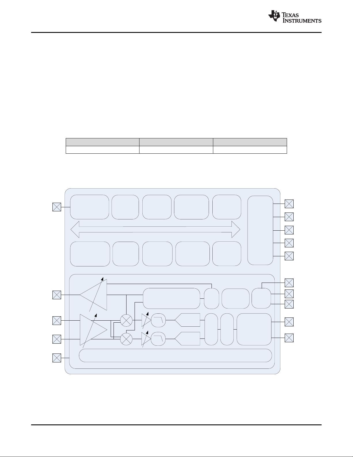
CC1120 High-Performance RF Transceiver for Narrowband Systems
1 Device Overview
1.1 Features
1
• High-Performance, Single-Chip Transceiver • Automatic Output Power Ramping
– Adjacent Channel Selectivity: • Configurable Data Rates: 0 to 200 kbps
64 dB at 12.5-kHz Offset
• Supported Modulation Formats: 2-FSK,
– Blocking Performance: 91 dB at 10 MHz 2-GFSK, 4-FSK, 4-GFSK, MSK, OOK
– Excellent Receiver Sensitivity: • WaveMatch: Advanced Digital Signal Processing
for Improved Sync Detect Performance
• –123 dBm at 1.2 kbps
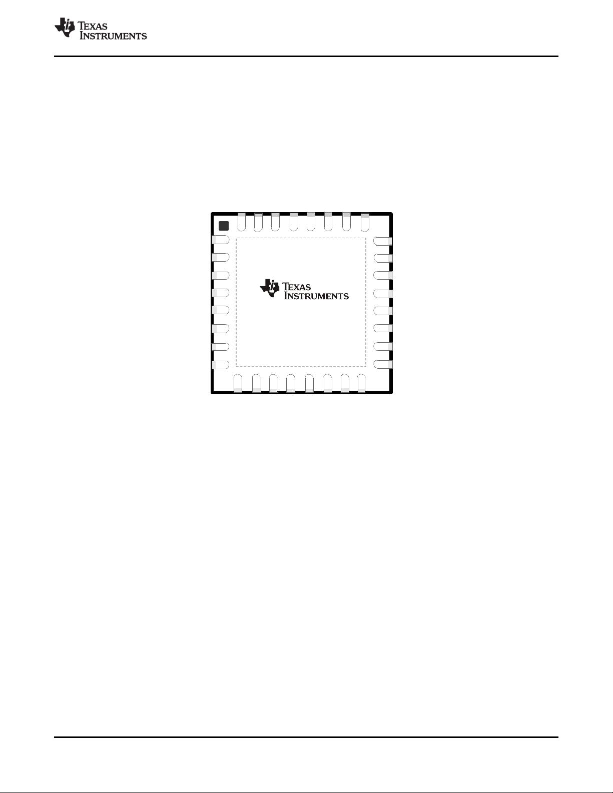
• RoHS-Compliant 5-mm × 5-mm No-Lead QFN
• –110 dBm at 50 kbps
32-Pin Package (RHB)
• –127 dBm Using Built-in Coding Gain
• Regulations – Suitable for Systems Targeting
– Very Low Phase Noise:
Compliance With
–111 dBc/Hz at 10-kHz Offset
– Europe: ETSI EN 300 220, ETSI EN 54-25
• Suitable for Systems Targeting ETSI Category 1
– US: FCC CFR47 Part 15, FCC CFR47 Part 90,
Compliance in 169-MHz and 433-MHz Bands
24, and 101
• High Spectral Efficiency (9.6 kbps in 12.5-kHz
– Japan: ARIB RCR STD-T30, ARIB STD-T67,
Channel in Compliance With FCC Narrowbanding
ARIB STD-T108
Mandate)
• Peripherals and Support Functions
• Separate 128-Byte RX and TX FIFOs
– Enhanced Wake-On-Radio (eWOR)
• Support for Seamless Integration With the CC1190
Functionality for Automatic Low-Power Receive
Device for Increased Range Giving up to 3-dB
Polling
Improvement in Sensitivity and up to +27-dBm
– Includes Functions for Antenna Diversity
Output Power
Support
• Power Supply
– Support for Retransmissions
– Wide Supply Voltage Range (2.0 V to 3.6 V)
– Support for Automatic Acknowledge of Received
– Low Current Consumption:
Packets
• RX: 2 mA in RX Sniff Mode
– TCXO Support and Control, Also in Power
• RX: 17 mA Peak Current in Low-Power
Modes
Mode
– Automatic Clear Channel Assessment (CCA) for
• RX: 22 mA Peak Current in
Listen-Before-Talk (LBT) Systems
High-Performance Mode
– Built-in Coding Gain Support for Increased
• TX: 45 mA at +14 dBm
Range and Robustness
– Power Down: 0.12 μA
– Digital RSSI Measurement
(0.5 μA With eWOR Timer Running)
– Temperature Sensor
• Programmable Output Power up to +16 dBm With
0.4-dB Step Size
1.2 Applications
• Narrowband Ultra-Low-Power Wireless Systems • IEEE 802.15.4g Systems
With Channel Spacing Down to
• Home and Building Automation
12.5 kHz
• Wireless Alarm and Security Systems
• 169-, 315-, 433-, 868-, 915-, 920-, 950-MHz
• Industrial Monitoring and Control
ISM/SRD Band
• Wireless Healthcare Applications
• Wireless Metering and Wireless Smart Grid
• Wireless Sensor Networks and Active RFID
(AMR and AMI)
• Private Mobile Radios
1
An IMPORTANT NOTICE at the end of this data sheet addresses availability, warranty, changes, use in safety-critical applications,
intellectual property matters and other important disclaimers. PRODUCTION DATA.
CC112X
MARC
Main Radio Control Unit
Ultra low power 16 bit
MCU
256 byte
FIFO RAM
buffer
4k byte
ROM
RF and DSP frontend
Packet handler
and FIFO control
Configuration and
status registers
eWOR
Enhanced ultra low power
Wake On Radio timer
SPI
Serial configuration
and data interface
Interrupt and
IO handler
System bus
PA
LNA_P
LNA_N
90dB dynamic
range ADC
90dB dynamic
range ADC
High linearity
LNA
14dBm high
efficiency PA
Channel
filter
XOSC
Cordic
AGC
Automatic Gain Control, 60dB VGA range
RSSI measurements and carrier sense detection
Highly flexible FSK / OOK
demodulator
(optional bit clock)
(optional low jitter serial
data output for legacy
protocols)
Data interface with
signal chain access
XOSC_Q1
XOSC_Q2
Ultra low power 32kHz
auto-calibrated RC oscillator
(optional 32kHz
clock intput)
CSn (chip select)
SI (serial input)
SO (serial output)
SCLK (serial clock)
(optional GPIO0-3)
Modulator
Fully integrated Fractional-N
Frequency Synthesizer
Output power ramping and OOK / ASK modulation
ifamp
ifamp
(optional autodetected
external XOSC / TCXO)
(optional GPIO for
antenna diversity)
I
Q
Battery sensor /
temp sensor
Power on reset
CC1120
SWRS112H –JUNE 2011–REVISED JULY 2015
www.ti.com
1.3 Description
The CC1120 device is a fully integrated single-chip radio transceiver designed for high performance at
very low-power and low-voltage operation in cost-effective wireless systems. All filters are integrated, thus
removing the need for costly external SAW and IF filters. The device is mainly intended for Industrial,
Scientific, and Medical (ISM) applications and Short Range Device (SRD) frequency bands at
164 to 192 MHz, 274 to 320 MHz, 410 to 480 MHz, and 820 to 960 MHz.
The CC1120 device provides extensive hardware support for packet handling, data buffering, burst
transmissions, clear channel assessment, link quality indication, and wake-on-radio. The main operating
parameters of the CC1120 device can be controlled through an SPI interface. In a typical system, the
CC1120 device is used with a microcontroller and only a few external passive components.
Device Information
(1)
PART NUMBER PACKAGE BODY SIZE (NOM)
CC1120 VQFN (32) 5.00 mm × 5.00 mm
(1) For more information, see Section 8, Mechanical Packaging and Orderable Information
1.4 Functional Block Diagram
Figure 1-1 shows the system block diagram of the CC1120 device.
Figure 1-1. Functional Block Diagram
2 Device Overview Copyright © 2011–2015, Texas Instruments Incorporated
Submit Documentation Feedback
Product Folder Links: CC1120
CC1120
www.ti.com
SWRS112H –JUNE 2011–REVISED JULY 2015
Table of Contents
4.14 Thermal Resistance Characteristics for RHB
1 Device Overview ......................................... 1
Package ............................................. 15
1.1 Features .............................................. 1
4.15 Timing Requirements ............................... 16
1.2 Applications........................................... 1
4.16 Regulatory Standards ............................... 16
1.3 Description............................................ 2
4.17 Typical Characteristics .............................. 17
1.4 Functional Block Diagram ............................ 2
5 Detailed Description ................................... 20
2 Revision History ......................................... 4
5.1 Block Diagram....................................... 20
3 Terminal Configuration and Functions.............. 5
5.2 Frequency Synthesizer.............................. 20
3.1 Pin Diagram .......................................... 5
5.3 Receiver............................................. 21
3.2 Pin Configuration ..................................... 6
5.4 Transmitter .......................................... 21
4 Specifications ............................................ 7
5.5 Radio Control and User Interface ................... 21
Absolute Maximum Ratings ................................. 7
5.6 Enhanced Wake-On-Radio (eWOR) ................ 21
4.1 ESD Ratings.......................................... 7
5.7 Sniff Mode........................................... 22
4.2 Recommended Operating Conditions (General
Characteristics) ....................................... 7 5.8 Antenna Diversity ................................... 22
4.3 RF Characteristics.................................... 7 5.9 WaveMatch.......................................... 23
4.4 Power Consumption Summary ....................... 8 6 Application, Implementation, and Layout ......... 24
4.5 Receive Parameters.................................. 9 6.1 Application Information .............................. 24
4.6 Transmit Parameters................................ 12 7 Device and Documentation Support ............... 26
4.7 PLL Parameters..................................... 13 7.1 Device Support ...................................... 26
4.8 32-MHz Clock Input (TCXO) ....................... 14 7.2 Documentation Support ............................. 27
4.9 32-MHz Crystal Oscillator ........................... 14 7.3 Trademarks.......................................... 27
4.10 32-kHz Clock Input.................................. 14 7.4 Electrostatic Discharge Caution..................... 27
4.11 32-kHz RC Oscillator ............................... 15 7.5 Glossary ............................................. 27
4.12 I/O and Reset ....................................... 15 8 Mechanical Packaging and Orderable
Information .............................................. 28
4.13 Temperature Sensor ................................ 15
Copyright © 2011–2015, Texas Instruments Incorporated Table of Contents 3
Submit Documentation Feedback
Product Folder Links: CC1120
CC1120
SWRS112H –JUNE 2011–REVISED JULY 2015
www.ti.com
2 Revision History
NOTE: Page numbers for previous revisions may differ from page numbers in the current version.
Changes from Revision G (September 2014) to Revision H Page
• Moved storage temperature range back to Absolute Maximum Ratings table ............................................... 7
• Updated the formatting of the Specifications section ........................................................................... 7
• Changed clock frequency minimum value FROM: 32 MHz TO: 31.25 MHz in 32-MHz Clock Input (TCXO) .......... 14
• Added clock frequency typical value of 32 MHz to 32-MHz Clock Input (TCXO) .......................................... 14
• Changed crystal frequency minimum value FROM: 32 MHz TO: 31.25 MHz in the 32-MHz Crystal Oscillator table . 14
• Added crystal frequency typical value of 32 MHz in the 32-MHz Crystal Oscillator table ................................. 14
• Changed table title FROM: Wakeup and Timing TO: Timing Requirements ............................................... 16
Changes from Revision F (July 2014) to Revision G Page
• Added " Ambient " to the temperature range condition and removed Tj from Temperature range ......................... 7
• Added data to TCXO table......................................................................................................... 14
4 Revision History Copyright © 2011–2015, Texas Instruments Incorporated
Submit Documentation Feedback
Product Folder Links: CC1120
CSn
SO (GPIO1)
DVDD
AVDD_IF
RBIAS
AVDD_RF
GPIO0
RESET_N
GPIO3
GPIO2
DVDD
VDD_GUARD
CC1120
5
4
3
2
1
LNA_P
LNA_N
DCPL_VCO
AVDD_SYNTH1
TRX_SW
19
20
21
22
23
AVDD_PFD_CHP
XOSC_Q2
XOSC_Q1
DCPL_PFD_CHP
27
28
29
30
31
DCPL
6
7
PA
18
17
26
25
15
9
10
11
12
13
14
SI
N.C.
DCPL_XOSC
AVDD_XOSC
8
SCLK
16
24
EXT_XOSC
32
LPF0
LPF1
AVDD_SYNTH2
GND
GROUND PAD
CC1120
www.ti.com
SWRS112H –JUNE 2011–REVISED JULY 2015
3 Terminal Configuration and Functions
3.1 Pin Diagram
Figure 3-1 shows pin names and locations for the CC1120 device.
Figure 3-1. Package 5-mm × 5-mm QFN
Copyright © 2011–2015, Texas Instruments Incorporated Terminal Configuration and Functions 5
Submit Documentation Feedback
Product Folder Links: CC1120
剩余34页未读,继续阅读
资源评论
不觉明了
- 粉丝: 3165
- 资源: 5429
上传资源 快速赚钱
- 我的内容管理 展开
- 我的资源 快来上传第一个资源
- 我的收益 登录查看自己的收益
- 我的积分 登录查看自己的积分
- 我的C币 登录后查看C币余额
- 我的收藏
- 我的下载
- 下载帮助
安全验证
文档复制为VIP权益,开通VIP直接复制
信息提交成功