没有合适的资源?快使用搜索试试~ 我知道了~
TI-DIR9001.pdf
需积分: 5 0 下载量 81 浏览量
2022-12-03
23:57:34
上传
评论 4
收藏 1019KB PDF 举报
温馨提示
试读
38页
TI-DIR9001.pdf
资源推荐
资源详情
资源评论
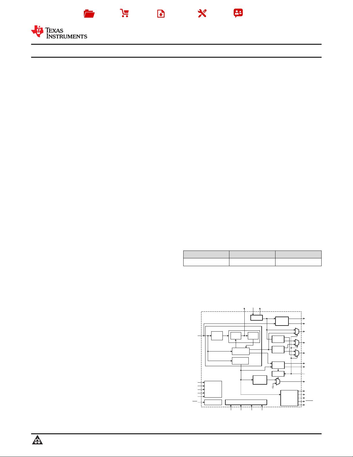
Clock and Data Recovery
SCKO
BCKO
LRCKO
DOUT
RXIN
Divider
FILT XTOXTI
FSOUT0
FSOUT1
RST
OSC
RESET
CLKST
EMPH
UOUT
COUT
BFRAME
VCO
CKSEL
DGND
ERROR
AUDIO
Power Supply
V
DD
DGND AGND
V
CC
PSCK0
PSCK1
FMT0
RSV
PLL
Divider
Decoder
FMT1
Preamble
Detector
Charge
Pump
Sampling
Frequency
Calculator
Clock
Decoder
Biphase
Data Decoder
Serial
AudioData
Formatter
ERROR
Detector
Function
Control
AudioData
MUTE Control
Channel Status
and
UserData
Output
Product
Folder
Sample &
Buy
Technical
Documents
Tools &
Software
Support &
Community
DIR9001
SLES198A –DECEMBER 2006–REVISED MAY 2015
DIR9001 96-kHz, 24-Bit Digital Audio Interface Receiver
1 Features 3 Description
The DIR9001 is a digital audio interface receiver that
1
• One-Chip Digital Audio Interface Receiver (DIR)
can receive a 28-kHz to 108-kHz sampling-
Including Low-Jitter Clock-Recovery System
frequency, 24-bit-data-word, biphase-encoded signal.
• Compliant With Digital Audio Interface Standards:
The DIR9001 complies with IEC60958-3, JEITA CPR-
IEC60958 (former IEC958), JEITA CPR-1205
1205 (Revised version of EIAJ CP-1201), AES3,
(former EIAJ CP-1201, CP-340), AES3, EBU
EBUtech3250, and it can be used in various
tech3250
applications that require a digital audio interface.
• Clock Recovery and Data Decode From Biphase
The DIR9001 supports many output system clock and
Input Signal, Generally Called S/PDIF, EIAJ CP-
output data formats and can be used flexibly in many
1201, IEC60958, AES/EBU
application systems. As the all functions which the
DIR9001 provides can be controlled directly through
• Biphase Input Signal Sampling Frequency (f
S
)
control pins, it can be used easily in an application
Range: 28 kHz to 108 kHz
system that does not have a microcontroller. Also, as
• Low-Jitter Recovered System Clock: 50 ps
dedicated pins are provided for the channel-status bit
• Jitter Tolerance Compliant With IEC60958-3
and user-data bit, processing of their information can
be easily accomplished by connecting with a
• Selectable Recovered System Clock: 128 f
S
,
microcontroller, DSP, or others.
256 f
S
, 384 f
S
, 512 f
S
• Serial Audio Data Output Formats: 24-Bit I
2
S;
The DIR9001 does not require an external clock
source or resonator for decode operation if the
MSB-First, 24-Bit Left-Justified; MSB-First 16-, 24-
internal actual-sampling-frequency calculator is not
Bit Right-Justified
used. Therefore, it is possible to reduce the cost of a
• User Data, Channel-Status Data Outputs
system.
Synchronized With Decoded Serial Audio Data
The operating temperature range of the DIR9001 is
• No External Clock Required for Decode
specified as –40°C to 85°C, which makes it suitable
• Includes Actual Sampling Frequency Calculator
for automotive applications.
(Needs External 24.576-MHz Clock)
• Function Control: Parallel (Hardware)
Device Information
PART NUMBER PACKAGE BODY SIZE (NOM)
• Functions Similar and Pin Assignments Equivalent
to Those of DIR1703
DIR9001 TSSOP (28) 4.40 mm × 9.70 mm
• Single Power Supply: 3.3 V (2.7 V to 3.6 V)
(1) For all available packages, see the orderable addendum at
the end of the data sheet.
• Wide Operating Temperature Range: –40°C to
85°C
• 5 V-Tolerant Digital Inputs
Block Diagram
• Package: 28-pin TSSOP, Pin Pitch: 0,65 mm
2 Applications
• AV/DVD Receiver, AV Amplifier
• Car or Mobile Audio System
• Digital Television
• Musical Instruments
• Recording Systems
• High-End Audio/Sound Card for PC
• Replacement of DIR1703
• Other Applications Requiring S/PDIF Receiver
1
An IMPORTANT NOTICE at the end of this data sheet addresses availability, warranty, changes, use in safety-critical applications,
intellectual property matters and other important disclaimers. PRODUCTION DATA.
DIR9001
SLES198A –DECEMBER 2006–REVISED MAY 2015
www.ti.com
Table of Contents
8.2 Functional Block Diagram ....................................... 11
1 Features.................................................................. 1
8.3 Feature Description................................................. 12
2 Applications ........................................................... 1
8.4 Device Functional Modes........................................ 20
3 Description ............................................................. 1
8.5 Programming........................................................... 23
4 Revision History..................................................... 2
9 Application and Information............................... 26
5 Device Comparison Table..................................... 3
9.1 Application Information............................................ 26
5.1 Differences From DIR1703 ....................................... 3
9.2 Typical Application .................................................. 27
6 Pin Configuration and Functions......................... 4
10 Power Supply Recommendations ..................... 29
7 Specifications......................................................... 6
11 Layout................................................................... 29
7.1 Absolute Maximum Ratings ...................................... 6
11.1 Layout Guidelines ................................................. 29
7.2 ESD Ratings.............................................................. 6
11.2 Layout Example .................................................... 30
7.3 Recommended Operating Conditions....................... 6
12 Device and Document Support.......................... 31
7.4 Thermal Information.................................................. 7
12.1 Community Resources.......................................... 31
7.5 Electrical Characteristics........................................... 7
12.2 Trademarks........................................................... 31
7.6 Timing Requirements................................................ 8
12.3 Electrostatic Discharge Caution............................ 31
7.7 Switching Characteristics.......................................... 9
12.4 Glossary................................................................ 31
7.8 Typical Characteristics............................................ 10
13 Mechanical, Packaging, and Orderable
8 Detailed Description............................................ 11
Information ........................................................... 31
8.1 Overview ................................................................. 11
4 Revision History
Changes from Original (Dec 2006) to Revision A Page
• Added Pin Configuration and Functions section, ESD Ratings table, Feature Description section, Device Functional
Modes, Application and Implementation section, Power Supply Recommendations section, Layout section, Device
and Documentation Support section, and Mechanical, Packaging, and Orderable Information section .............................. 1
2 Submit Documentation Feedback Copyright © 2006–2015, Texas Instruments Incorporated
Product Folder Links: DIR9001
DIR9001
www.ti.com
SLES198A –DECEMBER 2006–REVISED MAY 2015
5 Device Comparison Table
5.1 Differences From DIR1703
The DIR9001 has many improved functions compared to the DIR1703.
The DIR9001 functions are similar to those of the DIR1703.
The DIR9001 pin assignment is equivalent to that of the DIR1703.
The DIR9001 biphase input signal decoding function is almost equivalent to that of the DIR1703.
The differences between the DIR9001 and DIR1703 are shown in Table 1.
Table 1. Main Differences Between DIR1703 and DIR9001
DIFFERENCE DIR1703 DIR9001
Operational supply-voltage range 3 V to 3.6 V 2.7 V to 3.6 V
Operation temperature range –25°C to 85°C –40°C to 85°C
Package SSOP-28P, pin pitch: 0.65 mm TSSOP-28P, pin pitch: 0.65 mm
Clock recovery architecture SpAct™ feature Conventional PLL
IEC60958-3 jitter tolerance Not compliant Compliant
IEC60958 sampling frequency accuracy Level II (±1000 ppm) Level III (±12.5%)
Acceptable sampling frequency 32/44.1/48/88.2/96 kHz, ±1500 ppm 28 kHz to 108 kHz continuous
Biphase input signal level CMOS level 5-V tolerant TTL level
Connection of loop filter Between FILT pin and VCC Between FILT pin and AGND
XTI source clock frequency One of the following clock sources or Optional 24.576-MHz (24.576-MHz clock is
resonators must be connected to the XTI pin: only required to use the internal actual-
4.069/5.6448/6.144/ 8.192/11.2896/12.288/ sampling-frequency calculator or use the
16.384/16.9344/18.432/ 22.5792/24.576-MHz DIR9001 as a 24.576-MHz clock generator.)
BFRAME H period 32/f
S
8/f
S
Channel status and user data Synchronous with LRCK transition 17-BCK delay from LRCK transition
Latest tracked frequency hold Available Not available
PLL mode clock at error Latest tracked frequency VCO free-running frequency
Clock transition signal out CKTRNS pin, active H CLKST pin, active-high
Oscillation amplifier External feedback resistor (typ. 1 MΩ) Internal feedback resistor
The differences between the DIR1703 and DIR9001 I/O pins are shown in Table 2.
Table 2. The Differences Between DIR1703 and DIR9001 in All I/O Pin
PIN NO. DIR1703 DIR9001 DIFFERENCES DESCRIPTIONS OF DIR9001
1 ADFLG AUDIO Pin name only Channel-status data information of non-audio sample word, active-low
2 BRATE0 FSOUT0 Pin name only Actual-sampling-frequency calculated result output 0
3 BRATE1 FSOUT1 Pin name only Actual-sampling-frequency calculated result output 1
4 SCKO SCKO Same function System clock output
5 V
DD
V
DD
Same function Digital power supply, 3.3-V
6 DGND DGND Same function Digital ground
7 XTO XTO Same function Oscillation amplifier output
8 XTI XTI Same function Oscillation amplifier input, or external XTI source clock input
9 CKTRNS CLKST CLKST is active-high Clock change/transition signal output
10 LRCKO LRCKO Same function Audio data latch enable output
11 BCKO BCKO Same function Audio data bit clock output
12 DOUT DOUT Same function 16 bit–24 bit decoded serial digital audio data output
13 SCF0 PSCK0 Pin name only SCKO output frequency selection 0
14 SCF1 PSCK1 Pin name only SCKO output frequency selection 1
15 CSBIT COUT Pin name only Channel-status data serial output synchronized with LRCKO
Copyright © 2006–2015, Texas Instruments Incorporated Submit Documentation Feedback 3
Product Folder Links: DIR9001
8
7
6
5
4
3
2
1
AUDIO
FSOUT0
FSOUT1
SCKO
V
DD
DGND
XTO
XTI
CLKST
LRCKO
BCKO
DOUT
PSCK0
PSCK1
21
22
23
24
25
26
27
28
CKSEL
ERROR
FMT1
FMT0
V
CC
AGND
FILT
RST
RXIN
RSV
BFRAME
EMPH
UOUT
COUT
14
13
12
11
10
9
15
16
17
18
19
20
DIR9001
(TOP VIEW)
DIR9001
SLES198A –DECEMBER 2006–REVISED MAY 2015
www.ti.com
Table 2. The Differences Between DIR1703 and DIR9001 in All I/O Pin (continued)
PIN NO. DIR1703 DIR9001 DIFFERENCES DESCRIPTIONS OF DIR9001
16 URBIT UOUT Pin name only User data serial output synchronized with LRCKO
17 EMFLG EMPH Pin name only Channel-status data Information of pre-emphasis (50 μs/15 μs)
18 BFRAME BFRAME Same function Indication of top block of biphase input signal
19 BRSEL RSV Reserved Reserved, must be connected to DGND
20 DIN RXIN Pin name only Biphase digital data input
21 RST RST Same function Reset control input, active-low
22 FILT FILT Same function External filter connection terminal. Recommended filter must be connected.
23 AGND AGND Same function Analog ground
24 V
CC
V
CC
Same function Analog power supply, 3.3-V
25 FMT0 FMT0 Same function Decoded serial digital audio data output format selection 0
26 FMT1 FMT1 Same function Decoded serial digital audio data output format selection 1
27 UNLOCK ERROR Pin name only Indication of internal PLL or data parity error
28 CKSEL CKSEL Same function Selection of system clock source, Low: PLL (VCO) clock, High: XTI clock
6 Pin Configuration and Functions
4 Submit Documentation Feedback Copyright © 2006–2015, Texas Instruments Incorporated
Product Folder Links: DIR9001
DIR9001
www.ti.com
SLES198A –DECEMBER 2006–REVISED MAY 2015
Pin Functions
PIN
PULL
I/O REMARKS DESCRIPTION
UP/DOWN
NAME NO.
AGND 23 – Analog ground
AUDIO 1 OUT CMOS Channel-status data information of non-audio sample word, active-low
BCKO 11 OUT CMOS Audio data bit clock output
BFRAME 18 OUT CMOS Indication of top block of biphase input signal
CKSEL 28 IN Pulldown 5-V tolerant TTL Selection of system clock source, Low: PLL (VCO) clock, High: XTI clock
(1)
CLKST 9 OUT CMOS Clock change/transition signal output
COUT 15 OUT CMOS Channel-status data serial output synchronized with LRCKO
DGND 6 – Digital ground
DOUT 12 OUT CMOS 16-bit/24-bit decoded serial digital audio data output
EMPH 17 OUT CMOS Channel-status data information of pre-emphasis (50 μs/15 μs)
ERROR 27 OUT CMOS Indication of internal PLL or data parity error
FILT 22 – External filter connection terminal; must connect recommended filter.
FMT0 25 IN Pulldown 5-V tolerant TTL Decoded serial digital audio data output format selection 0
(1)
FMT1 26 IN Pulldown 5-V tolerant TTL Decoded serial digital audio data output format selection 1
(1)
FSOUT0 2 OUT CMOS Actual sampling frequency calculated result output 0
FSOUT1 3 OUT CMOS Actual sampling frequency calculated result output 1
LRCKO 10 OUT CMOS Audio data latch enable output
PSCK0 13 IN Pulldown 5-V tolerant TTL PLL source SCKO output frequency selection 0
(1)
PSCK1 14 IN Pulldown 5-V tolerant TTL PLL source SCKO output frequency selection 1
(1)
RST 21 IN Pullup 5-V tolerant TTL Reset control input, active-low
(2)
RSV 19 IN Pulldown Reserved, must be connected to DGND
(1)
RXIN 20 IN 5-V tolerant TTL Biphase digital data input
(3)
SCKO 4 OUT CMOS System clock output
UOUT 16 OUT CMOS User data serial output synchronized with LRCKO
V
CC
24 – Analog power supply, 3.3-V
V
DD
5 – Digital power supply, 3.3-V
CMOS
XTI 8 IN Oscillation amplifier input, or external XTI source clock input
Schmitt-trigger
XTO 7 OUT CMOS Oscillation amplifier output
(1) TTL Schmitt-trigger input with internal pulldown (51 kΩ typical), 5-V tolerant
(2) TTL Schmitt-trigger input with internal pullup (51 kΩ typical), 5-V tolerant
(3) TTL Schmitt-trigger input, 5-V tolerant.
Copyright © 2006–2015, Texas Instruments Incorporated Submit Documentation Feedback 5
Product Folder Links: DIR9001
剩余37页未读,继续阅读
资源评论
不觉明了
- 粉丝: 3153
- 资源: 5416
上传资源 快速赚钱
- 我的内容管理 展开
- 我的资源 快来上传第一个资源
- 我的收益 登录查看自己的收益
- 我的积分 登录查看自己的积分
- 我的C币 登录后查看C币余额
- 我的收藏
- 我的下载
- 下载帮助
安全验证
文档复制为VIP权益,开通VIP直接复制
信息提交成功