没有合适的资源?快使用搜索试试~ 我知道了~
TI-TS5N118.pdf
需积分: 5 0 下载量 98 浏览量
2022-12-01
23:56:43
上传
评论 4
收藏 1.1MB PDF 举报
温馨提示
试读
19页
TI-TS5N118.pdf
资源推荐
资源详情
资源评论
www.ti.com
FEATURES APPLICATIONS
1
2
3
4
5
6
7
8
16
15
14
13
12
11
10
9
B4
B3
B2
B1
A
NC
OE
GND
V
CC
B5
B6
B7
B8
S0
S1
S2
DBQ OR PW PACKAGE
(TOP VIEW)
NC − No internal connection
DESCRIPTION/ORDERING INFORMATION
TS5N118
1-OF-8 FET MULTIPLEXER/DEMULTIPLEXER
HIGH-BANDWIDTH BUS SWITCH
SCDS205 – AUGUST 2005
• PCI Interface
• Low and Flat ON-State Resistance (r
on
)
Characteristics Over Operating Range
• Differential Signal Interface
(r
on
= 3 Ω Typ)
• Memory Interleaving
• 0- to 10-V Switching on Data I/O Ports
• Bus Isolation
• Low-Distortion Signal Gating
• Bidirectional Data Flow With Near-Zero
Propagation Delay
• Low Input/Output Capacitance Minimizes
Loading and Signal Distortion
(C
io(OFF)
= 20 pF Max, B Port)
• V
CC
Operating Range From 4.75 V to 5.25 V
• Latch-Up Performance Exceeds 100 mA Per
JESD 78, Class II
• ESD Performance Tested Per JESD 22
– 2000-V Human-Body Model
(A114-B, Class II)
– 1000-V Charged-Device Model (C101)
• Supports Both Digital and Analog
Applications
The TS5N118 is a high-bandwidth FET bus switch utilizing a charge pump to elevate the gate voltage of the pass
transistor, providing a low and flat ON-state resistance (r
on
). The low and flat ON-state resistance allows for
minimal propagation delay and supports rail-to-rail switching on the data input/output (I/O) ports. The device also
features low data I/O capacitance to minimize capacitive loading and signal distortion on the data bus.
Specifically designed to support high-bandwidth applications, the TS5N118 provides an optimized interface
solution ideally suited for broadband communications, networking, and data-intensive computing systems.
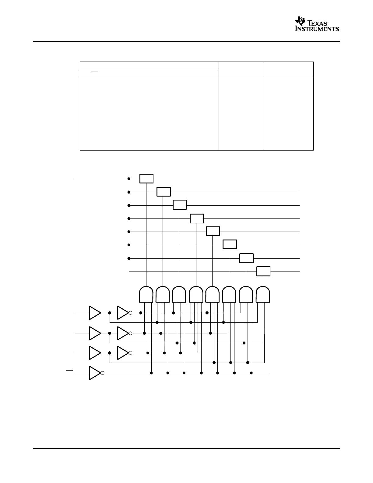
The TS5N118 is a 1-of-8 multiplexer/demultiplexer with a single output-enable ( OE) input. The select (S0, S1,
S2) inputs control the data path of the multiplexer/demultiplexer. When OE is low, the multiplexer/demultiplexer is
enabled and the A port is connected to the B port, allowing bidirectional data flow between ports. When OE is
high, the multiplexer/demultiplexer is disabled and a high-impedance state exists between the A and B ports.
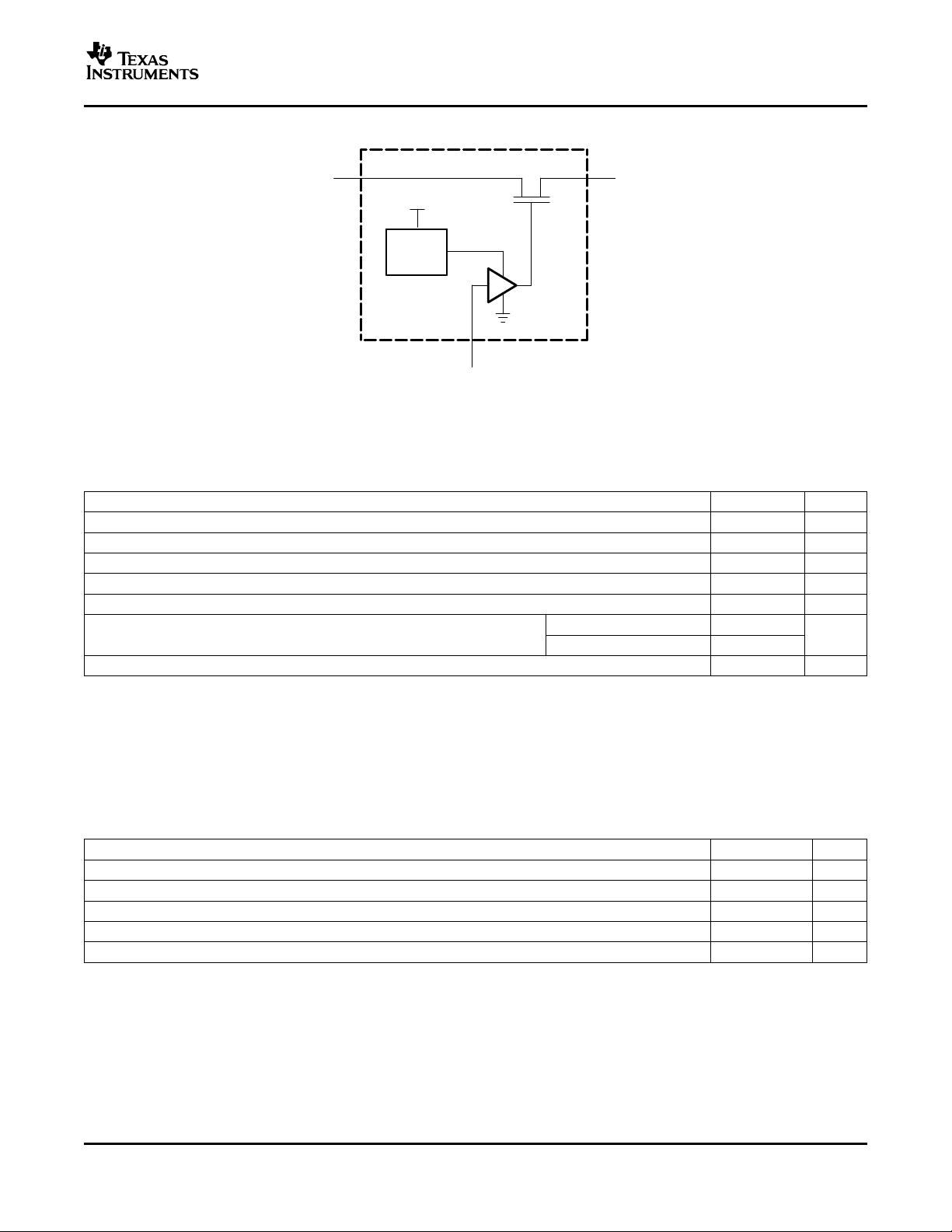
This device is fully specified for partial-power-down applications using I
off
. The I
off
circuitry prevents damaging
current backflow through the device when it is powered down. The device has isolation during power off.
To ensure the high-impedance state during power up or power down, OE should be tied to V
CC
through a pullup
resistor; the minimum value of the resistor is determined by the current-sinking capability of the driver.
ORDERING INFORMATION
T
A
PACKAGE
(1)
ORDERABLE PART NUMBER TOP-SIDE MARKING
SSOP (QSOP) – DBQ Tape and reel TS5N118DBQR
–40 ° C to 85 ° C YB118
TSSOP – PW Tape and reel TS5N118PWR
(1) Package drawings, standard packing quantities, thermal data, symbolization, and PCB design guidelines are available at
www.ti.com/sc/package.
Please be aware that an important notice concerning availability, standard warranty, and use in critical applications of Texas
Instruments semiconductor products and disclaimers thereto appears at the end of this data sheet.
PRODUCTION DATA information is current as of publication date.
Copyright © 2005, Texas Instruments Incorporated
Products conform to specifications per the terms of the Texas
Instruments standard warranty. Production processing does not
necessarily include testing of all parameters.
www.ti.com
B5
B1
A
S0
S1
S2
OE
B2
B3
B4
B6
B7
B8
SW
SW
SW
SW
SW
SW
SW
SW
5
11
10
9
7
4
3
2
1
15
14
13
12
TS5N118
1-OF-8 FET MULTIPLEXER/DEMULTIPLEXER
HIGH-BANDWIDTH BUS SWITCH
SCDS205 – AUGUST 2005
FUNCTION TABLE
INPUTS
INPUT/OUTPUT
FUNCTION
A
OE S2 S1 S0
L L L L B1 A port = B1 port
L L L H B2 A port = B2 port
L L H L B3 A port = B3 port
L L H H B4 A port = B4 port
L H L L B5 A port = B5 port
L H L H B6 A port = B6 port
L H H L B7 A port = B7 port
L H H H B8 A port = B8 port
H X X X Z Disconnect
LOGIC DIAGRAM (POSITIVE LOGIC)
2
www.ti.com
A
EN
(1)
B
(1) EN is the internal enable signal applied to the switch.
Charge
Pump
V
CC
Absolute Maximum Ratings
(1)
Recommended Operating Conditions
(1)
TS5N118
1-OF-8 FET MULTIPLEXER/DEMULTIPLEXER
HIGH-BANDWIDTH BUS SWITCH
SCDS205 – AUGUST 2005
SIMPLIFIED SCHEMATIC, EACH FET SWITCH (SW)
over operating free-air temperature range (unless otherwise noted)
MIN MAX UNIT
V
CC
Supply voltage range –0.5 7 V
V
IN
Control input voltage range
(2) (3)
–0.5 7 V
V
I/O
Switch I/O voltage range
(2) (3) (4)
–0.5 11 V
I
I/O
ON-state switch current
(5)
± 100 mA
Continuous current through V
CC
or GND ± 100 mA
DBQ package 90
θ
JA
Package thermal impedance
(6)
° C/W
PW package 108
T
stg
Storage temperature range –65 150 ° C
(1) Stresses beyond those listed under "absolute maximum ratings" may cause permanent damage to the device. These are stress ratings
only, and functional operation of the device at these or any other conditions beyond those indicated under "recommended operating
conditions" is not implied. Exposure to absolute-maximum-rated conditions for extended periods may affect device reliability.
(2) All voltages are with respect to ground, unless otherwise specified.
(3) The input and output voltage ratings may be exceeded if the input and output clamp-current ratings are observed.
(4) V
I
and V
O
are used to denote specific conditions for V
I/O
.
(5) I
I
and I
O
are used to denote specific conditions for I
I/O
.
(6) The package thermal impedance is calculated in accordance with JESD 51-7.
MIN MAX UNIT
V
CC
Supply voltage 4.75 5.25 V
V
IH
High-level control input voltage 2 5.25 V
V
IL
Low-level control input voltage 0 0.8 V
V
I/O
Data input/output voltage 0 10 V
T
A
Operating free-air temperature –40 85 ° C
(1) All unused inputs of the device must be held at V
CC
or GND to ensure proper device operation. Refer to the TI application report,
Implications of Slow or Floating CMOS Inputs, literature number SCBA004.
3
www.ti.com
Electrical Characteristics
(1)
Switching Characteristics
Dynamic Characteristics
TS5N118
1-OF-8 FET MULTIPLEXER/DEMULTIPLEXER
HIGH-BANDWIDTH BUS SWITCH
SCDS205 – AUGUST 2005
over recommended operating free-air temperature range (unless otherwise noted)
PARAMETER TEST CONDITIONS MIN TYP
(2)
MAX UNIT
I
IN
Control inputs V
CC
= 5.25 V, V
IN
= 0 to V
CC
10 µ A
V
O
= 0 to 10 V, Switch OFF, 10
V
CC
= 5.25 V,
V
I
= 0, V
IN
= V
CC
or GND
I
OZ
(3)
µ A
V
CC
= 0 V, V
O
= Open, V
I
= 0 to 10 V 10
I
I/O
= 0, 10
I
CC
V
CC
= 5.25 V, V
IN
= V
CC
or GND mA
Switch ON or OFF,
C
in
Control inputs V
CC
= 5 V, V
IN
= 10 V or 0 10 pF
Switch OFF, 120
A port V
CC
= 5 V, V
I/O
= 10 V or 0
V
IN
= V
CC
or GND,
C
io(OFF)
pF
Switch OFF, 20
B port V
CC
= 5 V, V
I/O
= 10 V or 0
V
IN
= V
CC
or GND,
Switch ON, 160
C
io(ON)
V
CC
= 5 V, V
I/O
= 10 V or 0 pF
V
IN
= V
CC
or GND,
V
I
= 0, I
O
= 50 mA 3 7.5
V
CC
= 4.75 V,
r
on
(4)
V
I
= 8 V, I
O
= –50 mA 7.5 Ω
TYP at V
CC
= 5 V
V
I
= 10 V, I
O
= –50 mA 12.5
(1) V
IN
and I
IN
refer to control inputs. V
I
, V
O
, I
I
, and I
O
refer to data pins
(2) All typical values are at V
CC
= 5 V (unless otherwise noted), T
A
= 25 ° C.
(3) For I/O ports, the parameter I
OZ
includes the I/O leakage current.
(4) Measured by the voltage drop between the A and B terminals at the indicated current through the switch. ON-state resistance is
determined by the lower of the voltages of the two (A or B) terminals.
over recommended operating free-air temperature range (unless otherwise noted) (see Figure 3 )
V
CC
= 5 V
FROM TO
± 0.25 V
PARAMETER UNIT
(INPUT) (OUTPUT)
MIN MAX
t
pd
(1)
A or B B or A 0.1 ns
t
pd(s)
S A 200 ns
S B 200
t
en
ns
OE A or B 200
S B 200
t
dis
ns
OE A or B 200
(1) The propagation delay is the calculated RC time constant of the typical ON-state resistance of the switch and the specified load
capacitance, when driven by an ideal voltage source (zero output impedance).
over recommended operating free-air temperature range, V
CC
= 5 V ± 5% (unless otherwise noted)
PARAMETER TEST CONDITIONS MIN TYP
(1)
MAX UNIT
Bandwidth (BW)
(2)
R
L
= 50 Ω , V
I
= 0.632 V (P-P), See Figure 4 25 MHz
OFF isolation (O
ISO
) R
L
= 50 Ω , V
I
= 0.632 V (P-P), f = 25 MHz, See Figure 5 –50 dB
Crosstalk (X
TALK
) R
L
= 50 Ω , V
I
= 0.632 V (P-P), f = 25 MHz, See Figure 6 –50 dB
(1) All typical values are at V
CC
= 5 V (unless otherwise noted), T
A
= 25 ° C.
(2) Bandwidth is the frequency at which the gain is –3 dB below the DC gain.
4
剩余18页未读,继续阅读
资源评论
不觉明了
- 粉丝: 3117
- 资源: 5348
上传资源 快速赚钱
- 我的内容管理 展开
- 我的资源 快来上传第一个资源
- 我的收益 登录查看自己的收益
- 我的积分 登录查看自己的积分
- 我的C币 登录后查看C币余额
- 我的收藏
- 我的下载
- 下载帮助
最新资源
- 筷手引流工具.apk
- 论文(最终)_20240430235101.pdf
- 基于python编写的Keras深度学习框架开发,利用卷积神经网络CNN,快速识别图片并进行分类
- 最全空间计量实证方法(空间杜宾模型和检验以及结果解释文档).txt
- 5uonly.apk
- 蓝桥杯Python组的历年真题
- 2023-04-06-项目笔记 - 第一百十九阶段 - 4.4.2.117全局变量的作用域-117 -2024.04.30
- 前端开发技术实验报告:内含4四实验&实验报告
- Highlight Plus v20.0.1
资源上传下载、课程学习等过程中有任何疑问或建议,欢迎提出宝贵意见哦~我们会及时处理!
点击此处反馈
安全验证
文档复制为VIP权益,开通VIP直接复制
信息提交成功