没有合适的资源?快使用搜索试试~ 我知道了~
TI-SN74HCS151.pdf
需积分: 5 0 下载量 162 浏览量
2022-11-28
23:26:42
上传
评论 4
收藏 1.41MB PDF 举报
温馨提示
试读
27页
TI-SN74HCS151.pdf
资源推荐
资源详情
资源评论
SN74HCS151 8-to-1 Multiplexer with Schmitt-Trigger Inputs
1 Features
• Wide operating voltage range: 2 V to 6 V
• Schmitt-trigger inputs allow for slow or noisy input
signals
• Low power consumption
– Typical I
CC
of 100 nA
– Typical input leakage current of ±100 nA
• ±7.8-mA output drive at 6 V
• Extended ambient temperature range: –40°C to
+125°C, T
A
2 Applications
• Data selection
• Multiplexing
3 Description
The SN74HCS151 is a data selector/multiplexer
containing full binary decoding to select one of eight
data sources and complementary outputs. The strobe
(G) input must be at a low logic level to enable the
inputs. A high level at the strobe terminal forces the W
output high and the Y output low.
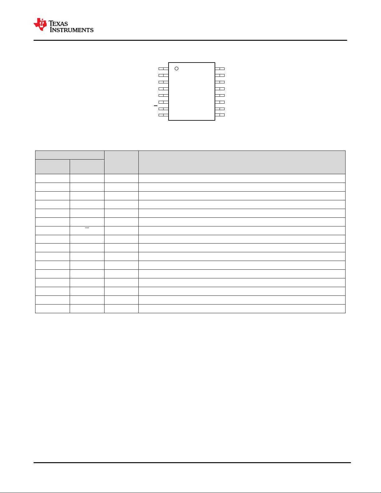
Device Information
PART NUMBER PACKAGE
(1)
BODY SIZE (NOM)
SN74HCS151PW TSSOP (16) 5.00 mm × 4.40 mm
SN74HCS151D SOIC (16) 9.90 mm × 3.90 mm
(1) For all available packages, see the orderable addendum at
the end of the data sheet.
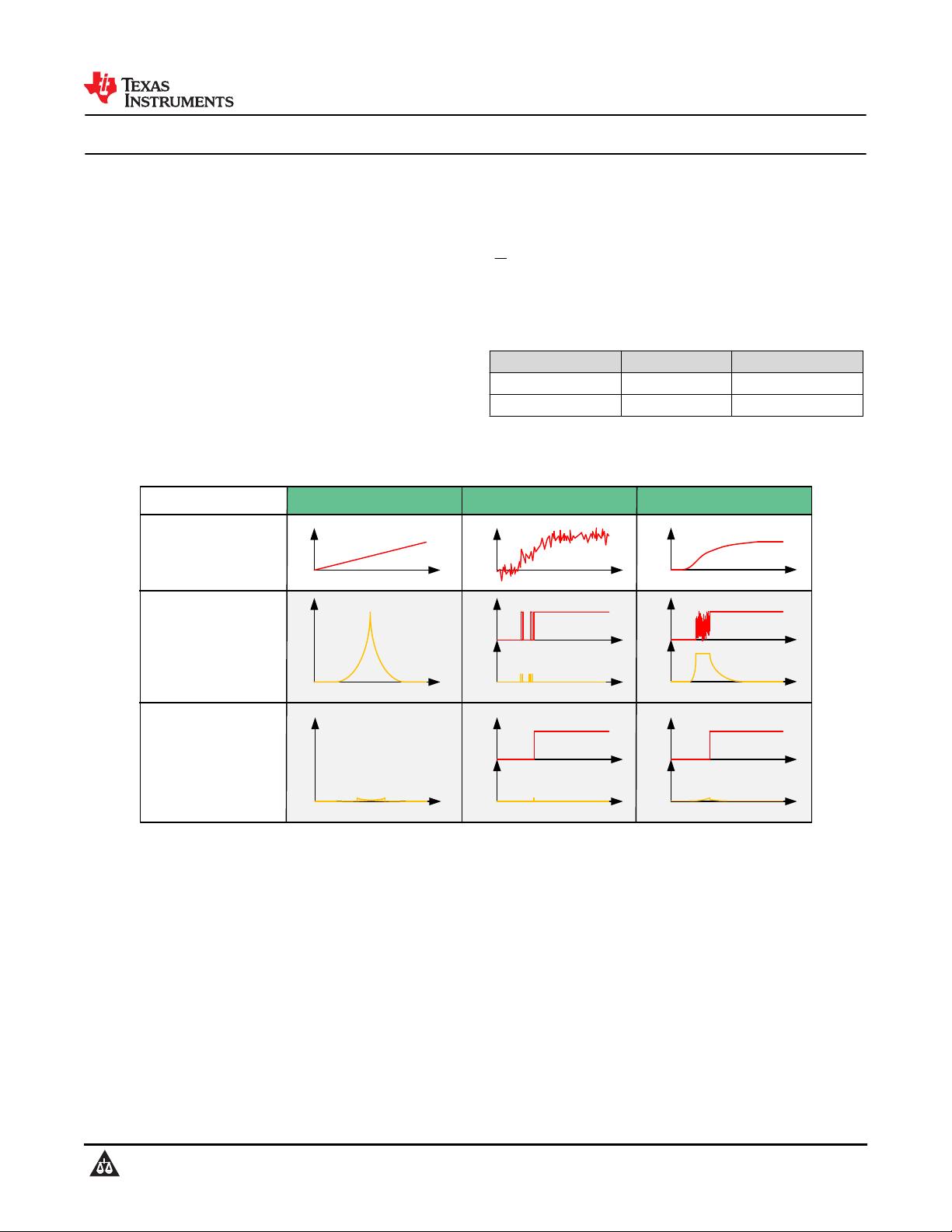
Input Voltage
Supply Current
Schmitt-trigger
CMOS Input
Response
Waveforms
Standard
CMOS Input
Response
Waveforms
Input Voltage
Supply Current
Input
Voltage
Input Voltage Time
Current
Output
Voltage
Current
Output
Voltage
Input
Voltage
Time
Current
Output
VoltageCurrent
Output
Voltage
Input
Voltage
Input Voltage
Waveforms
Low Power Noise Rejection
Supports Slow Inputs
Time
Time
Time
Time
Benefits of Schmitt-trigger inputs
www.ti.com
SN74HCS151
SCLS845A – SEPTEMBER 2020 – REVISED OCTOBER 2020
Copyright © 2020 Texas Instruments Incorporated
Submit Document Feedback
1
Product Folder Links: SN74HCS151
SN74HCS151
SCLS845A – SEPTEMBER 2020 – REVISED OCTOBER 2020
An IMPORTANT NOTICE at the end of this data sheet addresses availability, warranty, changes, use in safety-critical applications,
intellectual property matters and other important disclaimers. PRODUCTION DATA.
Table of Contents
1 Features............................................................................1
2 Applications..................................................................... 1
3 Description.......................................................................1
4 Revision History.............................................................. 2
5 Pin Configuration and Functions...................................3
6 Specifications.................................................................. 4
6.1 Absolute Maximum Ratings ....................................... 4
6.2 ESD Ratings .............................................................. 4
6.3 Recommended Operating Conditions ........................4
6.4 Thermal Information ...................................................4
6.5 Electrical Characteristics ............................................6
6.6 Switching Characteristics ...........................................6
6.7 Operating Characteristics .......................................... 7
6.8 Typical Characteristics................................................ 8
7 Parameter Measurement Information............................ 9
8 Detailed Description......................................................10
8.1 Overview................................................................... 10
8.2 Functional Block Diagram......................................... 10
8.3 Feature Description...................................................10
8.4 Device Functional Modes..........................................12
9 Application and Implementation.................................. 13
9.1 Application Information............................................. 13
9.2 Typical Application.................................................... 13
10 Power Supply Recommendations..............................16
11 Layout........................................................................... 16
11.1 Layout Guidelines................................................... 16
11.2 Layout Example...................................................... 16
12 Device and Documentation Support..........................17
12.1 Documentation Support.......................................... 17
12.2 Receiving Notification of Documentation Updates..17
12.3 Support Resources................................................. 17
12.4 Trademarks.............................................................17
12.5 Electrostatic Discharge Caution..............................17
12.6 Glossary..................................................................17
13 Mechanical, Packaging, and Orderable
Information.................................................................... 18
4 Revision History
NOTE: Page numbers for previous revisions may differ from page numbers in the current version.
Changes from September 28, 2020 to October 30, 2020 (from Revision * (September 2020) to
Revision A (October 2020)) Page
• Removed fmax and updated Transition-time in Switching Characteristics table................................................ 6
SN74HCS151
SCLS845A – SEPTEMBER 2020 – REVISED OCTOBER 2020
www.ti.com
2 Submit Document Feedback
Copyright © 2020 Texas Instruments Incorporated
Product Folder Links: SN74HCS151
5 Pin Configuration and Functions
1
2
3
7
4
5
6
14
13
12
8
11
10
9
GND
D5
D7
A
V
CC
15
16
D3
D2
D1
D0
Y
W
G
D4
C
D6
B
D or PW Package 16-Pin SOIC or TSSOP Top View
Pin Functions
PIN
I/O
(1)
DESCRIPTION
SOIC or
TSSOP NO.
NAME
1 D3 I Data input 3
2 D2 I Data input 2
3 D1 I Data input 1
4 D0 I Data input 0
5 Y O Data output
6 W O Data output, inverted
7 G I Output strobe, active low
8 GND — Ground
9 C I Address select C
10 B I Address select B
11 A I Address select A
12 D7 I Data input 7
13 D6 I Data input 6
14 D5 I Data input 5
15 D4 I Data input 4
16 V
CC
— Positive supply
www.ti.com
SN74HCS151
SCLS845A – SEPTEMBER 2020 – REVISED OCTOBER 2020
Copyright © 2020 Texas Instruments Incorporated
Submit Document Feedback
3
Product Folder Links: SN74HCS151
6 Specifications
6.1 Absolute Maximum Ratings
over operating free-air temperature range (unless otherwise noted)
(1)
MIN MAX UNIT
V
CC
Supply voltage –0.5 7 V
I
IK
Input clamp current
(2)
V
I
< –0.5 V or V
I
> V
CC
+ 0.5 V ±20 mA
I
OK
Output clamp current
(2)
V
I
< –0.5 V or V
I
> V
CC
+ 0.5 V ±20 mA
I
O
Continuous output current V
O
= 0 to V
CC
±35 mA
Continuous current through V
CC
or GND ±70 mA
T
J
Junction temperature
(3)
150 °C
T
stg
Storage temperature –65 150 °C
(1) Stresses beyond those listed under Absolute Maximum Rating may cause permanent damage to the device. These are stress ratings
only, which do not imply functional operation of the device at these or any other conditions beyond those indicated under
Recommended Operating Condition. Exposure to absolute-maximum-rated conditions for extended periods may affect device
reliability.
(2) The input and output voltage ratings may be exceeded if the input and output current ratings are observed.
(3) Guaranteed by design.
6.2 ESD Ratings
VALUE UNIT
V
(ESD)
Electrostatic discharge
Human-body model (HBM), per ANSI/ESDA/
JEDEC JS-001
(1)
±4000
V
Charged-device model (CDM), per JEDEC
specification JESD22-C101
(2)
±1500
(1) JEDEC document JEP155 states that 500-V HBM allows safe manufacturing with a standard ESD control process.
(2) JEDEC document JEP157 states that 250-V CDM allows safe manufacturing with a standard ESD control process.
6.3 Recommended Operating Conditions
over operating free-air temperature range (unless otherwise noted)
MIN NOM MAX UNIT
V
CC
Supply voltage 2 5 6 V
V
I
Input voltage 0 V
CC
V
V
O
Output voltage 0 V
CC
V
T
A
Ambient temperature –40 125 °C
6.4 Thermal Information
THERMAL METRIC
(1)
SN74HCS151
UNITPW (TSSOP) D (SOIC)
16 PINS 16 PINS
R
θJA
Junction-to-ambient thermal resistance 141.2 122.2 °C/W
R
θJC(top)
Junction-to-case (top) thermal resistance 78.8 80.9 °C/W
R
θJB
Junction-to-board thermal resistance 85.8 80.6 °C/W
Ψ
JT
Junction-to-top characterization parameter 27.7 40.4 °C/W
Ψ
JB
Junction-to-board characterization parameter 85.5 80.3 °C/W
SN74HCS151
SCLS845A – SEPTEMBER 2020 – REVISED OCTOBER 2020
www.ti.com
4 Submit Document Feedback
Copyright © 2020 Texas Instruments Incorporated
Product Folder Links: SN74HCS151
THERMAL METRIC
(1)
SN74HCS151
UNITPW (TSSOP) D (SOIC)
16 PINS 16 PINS
R
θJC(bot)
Junction-to-case (bottom) thermal resistance N/A N/A °C/W
(1) For more information about traditional and new thermal metrics, see the Semiconductor and IC Package Thermal Metrics application
report.
www.ti.com
SN74HCS151
SCLS845A – SEPTEMBER 2020 – REVISED OCTOBER 2020
Copyright © 2020 Texas Instruments Incorporated
Submit Document Feedback
5
Product Folder Links: SN74HCS151
剩余26页未读,继续阅读
资源评论
不觉明了
- 粉丝: 3125
- 资源: 5370
上传资源 快速赚钱
- 我的内容管理 展开
- 我的资源 快来上传第一个资源
- 我的收益 登录查看自己的收益
- 我的积分 登录查看自己的积分
- 我的C币 登录后查看C币余额
- 我的收藏
- 我的下载
- 下载帮助
安全验证
文档复制为VIP权益,开通VIP直接复制
信息提交成功