没有合适的资源?快使用搜索试试~ 我知道了~
TI-UCD3138128A.pdf
需积分: 9 0 下载量 155 浏览量
2022-11-21
23:23:32
上传
评论 5
收藏 2.36MB PDF 举报
温馨提示
试读
82页
TI-UCD3138128A.pdf
资源详情
资源评论
Product
Folder
Order
Now
Technical
Documents
Tools &
Software
Support &
Community
An IMPORTANT NOTICE at the end of this data sheet addresses availability, warranty, changes, use in safety-critical applications,
intellectual property matters and other important disclaimers. PRODUCTION DATA.
UCD3138128A
SLUSC99A –JULY 2016–REVISED JANUARY 2017
UCD3138128A Highly-Integrated Digital Controller For Isolated Power
1
1 Features
1
• 128 kB Program Flash Derivative of UCD3138xA
Family
– 4-32 kB Program Flash Memory Banks
– Supports Execution From 1 Bank, While
Programming Another
– Capability to Update Firmware Without
Shutting Down the Power Supply
– Additional Communication Ports Compared to
the UCD3138xA (+1 SPI, +1 I2C)
– Boot Flash Based Dual Memory Image
Support for ‘On the Fly’ Firmware Updates
• Synchronous Rectifier Dead Time Optimization
Peripheral to Use with UCD7138 Synchronous
Rectifier Driver
• Digital Control of up to 3 Independent Feedback
Loops
– Dedicated PID Based Hardware
– 2-pole/2-zero Configurable, Non-Linear Control
• Up to 16 MSPS Error A/D Converter (EADC)
– Configurable Resolution (min: 1 mV/LSB)
– Up to 8x Oversampling and Adaptive Sample
Positioning
– Hardware Based Averaging (up to 8x)
– 14 bit Effective Reference DAC
• Up to 8 High Resolution Digital Pulse Width
Modulated (DPWM) Outputs
– 250 ps Pulse Width Resolution
– 4 ns Frequency and Phase Resolution
– Adjustable Phase Shift and Dead-bands
– Cycle-by-Cycle Duty Cycle Matching
– Up to 2 MHz Switching Frequency
• Configurable Trailing/Leading/Triangular
Modulation
• RTC Support
• External Crystal Interface
• Configurable Feedback Control
– Voltage, Average Current and Peak Current
Mode Control
– Constant Current, Constant Power
• Configurable FM, Phase Shift Modulation and
PWM
• Fast, Automatic and Smooth Mode Switching
– Frequency Modulation and PWM
– Phase Shift Modulation and PWM
• High Efficiency and Light Load Management
– Burst Mode and Ideal Diode Emulation
– Synchronous Rectifier Soft On/Off
– Low IC Standby Power
• Primary Side Voltage Sensing
• Current Share (Average and Master/Slave)
• Feature Rich Fault Protection Options
– 7 Analog / 4 Digital Comparators,
– Cycle-by-Cycle Current Limiting
– Programmable Blanking Time and Fault
Counting
– External Fault Inputs
• Synchronization of DPWM Waveforms Between
Multiple UCD3138x Devices
• 15 channel, 12 bit, 539 ksps General Purpose
ADC
• Internal Temperature Sensor
• Fully Programmable High-Performance 31.25
MHz, 32-bit ARM7TDMI-S Processor
– 128 kB Program Flash (4-32 kB Banks)
– 2 kB Data Flash with ECC
– 8 kB Data RAM
– 8 kB Boot ROM Enables Firmware Boot-Load\
• Communication Peripherals,
– 2 - I
2
C/PMBus interfaces
– 2 - UARTs, 1 - SPI
• UART Auto Baud Rate Adjustment
• Timer Capture with Selectable Input Pins
• 80-pin QFP Package
• Operating Temperature: –40°C to 125°C
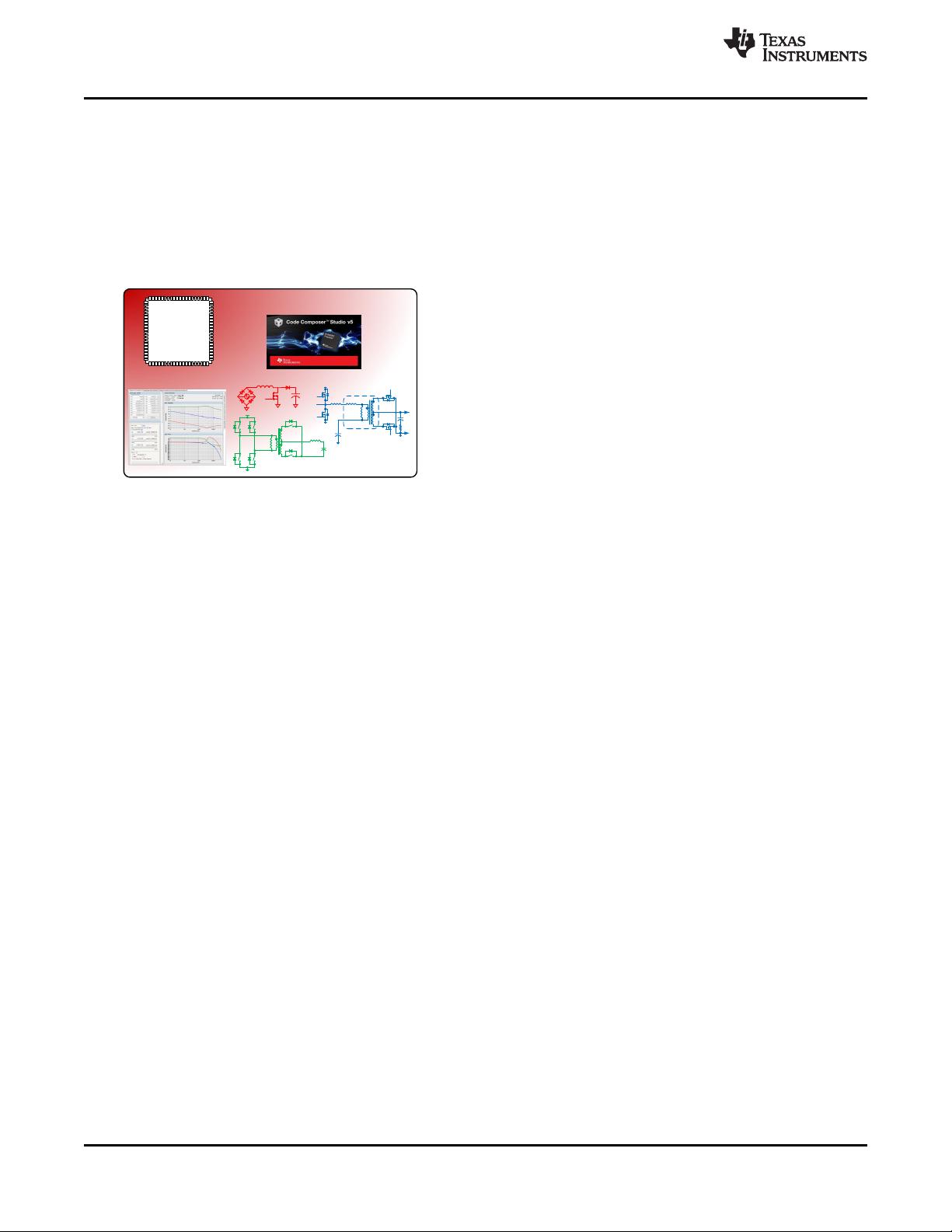
• Debug Interface
– Code Composer Studio with JTAG Interface
– Fusion Digital Power Designer GUI Support
UCD3138128A
Best in Class Firmware
Development Tools
Advanced Configuration &
Debug Tools
Advanced Topology Control
+ Forward, Flyback,
Half-bridge, etc...
Q
1
Q
3
Q
2
Q
4
V
IN
n
1
L
M
n
2
n
2
SR
2
SR
1
L
0
C
0
Q1
C
R
L
M
L
K
Q2
V
IN
Transformer
C
O
Q4
Q3
L
R
esr
Copyright © 2016, Texas Instruments Incorporated
2
UCD3138128A
SLUSC99A –JULY 2016–REVISED JANUARY 2017
www.ti.com
Product Folder Links: UCD3138128A
Submit Documentation Feedback Copyright © 2016–2017, Texas Instruments Incorporated
2 Applications
• Power Supplies and Telecom Rectifiers
• Power Factor Correction
• Isolated DC-DC Modules
• Phase Shifted Full Bridge with Peak Current Mode
Control, LLC, HSFB, Forward
Typical Applications and Tools
3 Description
The UCD3138xA is a digital power supply controller from Texas Instruments offering superior levels of integration
and performance in a single chip solution. The UCD3138128A offers 128 kB of program flash memory in
comparison to 32 kB in UCD3138A. and it also provides additional options for communication such as SPI and a
second I
2
C/PMBus port. The availability of of program Flash memory in multiple 32 kB banks enables designers
to implement dual images of firmware (that is, one main image + one back-up image) in the device and provides
the option to execute from either of the banks using appropriate algorithms. It also creates the unique opportunity
for the processor to load a new program and subsequently execute that program without interrupting power
delivery. This feature allows the end user to add new features to the power supply in the field while eliminating
any down-time required to load the new program.
The flexible nature of the UCD3138xA family makes it suitable for a wide variety of power conversion
applications. In addition, multiple peripherals inside the device have been specifically optimized to enhance the
performance of AC/DC and isolated DC/DC applications and reduce the solution component count in the IT and
network infrastructure space. The UCD3138xA family is a fully programmable solution offering customers
complete control of their application, along with ample flexibility for many solutions. At the same time, TI is
committed to simplifying our customer’s development effort through offering best in class development tools,
including application firmware, Code Composer Studio
TM
software development environment, and TI’s Fusion
Power Development GUI which enables customers to configure and monitor key system parameters.
At the core of the controller are the Digital Power Peripherals (DPP). Each DPP implements a high speed digital
control loop consisting of a dedicated Error Analog to Digital Converter (EADC), a PID based 2 pole - 2 zero
digital compensator and DPWM outputs with 250 ps pulse width resolution. The device also contains a 12-bit,
539 ksps general purpose ADC with up to 15 channels, timers, interrupt control, PMBus, I
2
C, SPI and UART
communications ports. The device is based on a 32-bit ARM7TDMI-S RISC microcontroller that performs real-
time monitoring, configures peripherals and manages communications. The ARM microcontroller executes its
program out of programmable flash memory as well as on chip RAM and ROM.
In addition to the DPP, specific power management peripherals have been added to enable high efficiency
across the entire operating range, high integration for increased power density, reliability, and lowest overall
system cost and high flexibility with support for the widest number of control schemes and topologies. Such
peripherals include: light load burst mode, synchronous rectification, LLC and phase shifted full bridge mode
switching, input voltage feed forward, copper trace current sense, ideal diode emulation, constant current
constant power control, synchronous rectification soft on and off, peak current mode control, flux balancing,
secondary side input voltage sensing, high resolution current sharing, hardware configurable soft start with pre
bias, as well as several other features. Topology support has been optimized for voltage mode and peak current
mode controlled phase shifted full bridge, single and dual phase PFC, bridgeless PFC, hard switched full bridge
and half bridge, active clamp forward converter, two switch forward converter and LLC half bridge and full bridge.
3
UCD3138128A
www.ti.com
SLUSC99A –JULY 2016–REVISED JANUARY 2017
Product Folder Links: UCD3138128A
Submit Documentation FeedbackCopyright © 2016–2017, Texas Instruments Incorporated
(1) For detailed ordering information please check the Mechanical, Packaging, and Orderable Information section at the end of this
datasheet.
The UCD3138128A is a functional variant of the UCD3138 Digital Power Controller that includes significant
improvements over the UCD3138. For a description of the complete changes made in the UCD3138128A, refer
to UCD3138128A Migration Guide. The major improvements are:
• The General Purpose ADC has been improved for better accuracy and performance at extreme cold
temperatures (–40°C).
• The UART peripheral has been modified to include a hardware based auto-baud rate adjustment feature.
• A new Synchronous Rectifier Dead Time Optimization hardware peripheral has been added. Benefits include:
– Improved efficiency
– Reduced synchronous rectifier voltage stresses
– Shorter development cycle
• A Duty Cycle Read Function has been added to improve use in peak current mode.
Device Information
(1)
PART NUMBER PACKAGE BODY SIZE (NOM)
UCD3138128A TQFP (80) 12.00 mm × 12.00 mm
4
UCD3138128A
SLUSC99A –JULY 2016–REVISED JANUARY 2017
www.ti.com
Product Folder Links: UCD3138128A
Submit Documentation Feedback Copyright © 2016–2017, Texas Instruments Incorporated
Table of Contents
1 Features.................................................................. 1
2 Applications ........................................................... 2
3 Description ............................................................. 2
4 Revision History..................................................... 4
5 Device Comparison ............................................... 5
6 Pin Configuration and Functions......................... 7
7 Specifications......................................................... 9
7.1 Absolute Maximum Ratings ...................................... 9
7.2 ESD Ratings.............................................................. 9
7.3 Recommended Operating Conditions..................... 10
7.4 Thermal Information................................................ 10
7.5 Electrical Characteristics......................................... 10
7.6 Timing Characteristics............................................. 13
7.7 PMBus/SMBus/I
2
C Timing...................................... 14
7.8 Typical Characteristics............................................ 15
7.9 Timing Diagrams..................................................... 16
8 Parametric Measurement Information ............... 17
8.1 Typical Clock Gating Power Savings...................... 18
9 Detailed Description............................................ 19
9.1 Overview ................................................................. 19
9.2 Functional Block Diagram ....................................... 21
9.3 Feature Description................................................. 22
9.4 Device Functional Modes........................................ 50
9.5 Register Maps......................................................... 57
10 Applications and Implementation...................... 60
10.1 Application Information.......................................... 60
10.2 Typical Application ............................................... 61
11 Power Supply Recommendations ..................... 72
12 Layout................................................................... 72
12.1 Device Grounding and Layout Guidelines ............ 72
12.2 Layout Examples................................................... 73
13 Device and Documentation Support ................. 74
13.1 Device Support...................................................... 74
13.2 Documentation Support ........................................ 74
13.3 Receiving Notification of Documentation Updates 76
13.4 Trademarks........................................................... 76
13.5 Electrostatic Discharge Caution............................ 76
13.6 Glossary................................................................ 76
14 Mechanical, Packaging, and Orderable
Information ........................................................... 76
4 Revision History
NOTE: Page numbers for previous revisions may differ from page numbers in the current version.
Changes from Original (June 2016) to Revision A Page
• Added two temperature ranges to the Internal oscillator frequency section. ....................................................................... 13
• Changed Figure 15 .............................................................................................................................................................. 29
• Changed Figure 35 to include DTC Adjustment .................................................................................................................. 51
• Changed capacitor from RESET to ground value from 0.22 µF to 2.2 µF. ......................................................................... 72
• Added updated V33 slew rate values in the Device Grounding and Layout Guidelines section. ........................................ 72
• Added bullet on unused GPIO pins ..................................................................................................................................... 72
• Changed "A" to part number ............................................................................................................................................... 73
UCD3138128A
www.ti.com
SLUSC99A –JULY 2016–REVISED JANUARY 2017
5
Product Folder Links: UCD3138128A
Submit Documentation FeedbackCopyright © 2016–2017, Texas Instruments Incorporated
(1) Represents an alternate pin out that is programmable via firmware.
5 Device Comparison
Table 1. Product Family Comparison
UCD
FEATURE
3138
3138A
RHA/RMH
3138064
3138064A
RMH
3138
3138A
RGC
3138064
3138064A
RGC
3138064
RGZ
3138128
3138128A
PFC
3138A64
PFC
Package Offering
40 Pin QFN
(6mm x 6mm)
40 Pin QFN
(6mm x 6mm)
64 Pin QFN
( 9mm x 9mm)
64 Pin QFN
(9mm x 9mm)
48 Pin QFN
(7mm x 7mm)
80 Pin QFP
(14mm x 14mm)
(Includes leads)
80 Pin QFP
(14mm x 14mm)
(Includes leads)
ARM7TDMI-S Core Processor 31.25 MHz 31.25 MHz 31.25 MHz 31.25 MHz 31.25 MHz 31.25 MHz 31.25 MHz
High Resolution DPWM Outputs (250ps Resolution) 8 8 8 8 8 8 8
Number of High Speed Independent Feedback Loops
(# Regulated Output Voltages
3 3 3 3 3 3 3
12-bit, 256kps, General Purpose ADC Channels 7 7 14 14 9 15 15
Digital Comparators at ADC Outputs 4 4 4 4 4 4 4
Flash Memory (Program) 32 kB 64 kB 32 kB 64 kB 64 kB 128 kB 64 kB
Number of Memory 32kB Flash Memory Banks 1 2 1 2 2 4
Only 1 bank of 64 kB
Flash available
Flash Memory (Data) 2 kB 2 kB 2 kB 2 kB 2 kB 2 kB 2 kB
RAM 4 kB 4 kB 4 kB 4 kB 4 kB 8 kB 8 kB
Programmable Fault Inputs 1 + 2
(1)
1 + 2
(1)
4 2 + 2
(1)
1 + 2
(1)
4 4
High Speed Analog Comparators with Cycle-by-Cycle
Current Limiting
6 6 7 7 6 7 7
UART (SCI) 1
(1)
1
(1)
2 2 2 2 2
PMBus/I
2
C
1 1 1 1 1 1 1
Additional I
2
C
0 0 0 1
(1)
1
(1)
1 1
SPI 0 0 0 1
(1)
1
(1)
1 1
Timers
4 (16 bit) and
1 (24 bit)
4 (16 bit) and
1 (24 bit)
4 (16 bit) and
1 (24 bit)
4 (16 bit) and
1 (24 bit)
4 (16 bit) and
1 (24 bit)
4 (16 bit) and
2 (24 bit)
4 (16 bit) and
2 (24 bit)
Timer PWM Outputs 1
(1)
1
(1)
2 2 1
(1)
4 4
Timer Capture Inputs 2
(1)
2
(1)
1 + 3
(1)
1 + 3
(1)
2
(1)
2 + 2
(1)
2 + 2
(1)
Total Digital GPIOs 18 18 30 30 24 43 43
External Interrupts 0 0 1 1 0 1 1
External Crystal Clock Support no no no no no Yes (pins #61, 62) Yes (pins #61, 62)
Peak Current Mode Control EADC2 Only All EADC channels EADC Only All EADC channels All EADC Channels All EADC Channels All EADC Channels
剩余81页未读,继续阅读
安全验证
文档复制为VIP权益,开通VIP直接复制
信息提交成功
评论0
最新资源