
具有诊断功能的 LP87702 双路降压转换器和 5V 升压转换器
1 特性
• 提供 FMEDA 和《功能安全手册》,可支持最高
SIL-2 (IEC 61508) 级别的系统级功能安全要求
• 两个高效降压直流/直流转换器:
– 最大输出电流 3.5A
– 2MHz、3MHz 或 4MHz 开关频率
– 自动 PWM/PFM 和强制 PWM 工作模式
– 输出电压范围为 0.7V 至 3.36V
• 5V 600mA 升压转换器
• 用于外部电压监控的两个输入
• 两个可编程电源正常信号
• 用于诊断的专用基准电压
• 支持复位输出的窗口看门狗
• 外部时钟输入,用于同步
• 扩频调制
• 可通过使能信号实现可编程启动和关断延迟与排序
• 可配置通用输出 (GPO)
• I2C 兼容接口,支持标准 (100kHz)、快速
(400kHz)、快速+ (1MHz) 和高速 (3.4MHz) 模式
• 具有可编程屏蔽的中断功能
• 输出短路和过载保护
• 过热警告和保护
• 过压保护 (OVP) 和欠压锁定 (UVLO)
2 应用
• 楼宇自动化:
– 自动门
– 运动检测器(PIR/运动传感器)
– 视频监控:
• 占位检测(人员跟踪、人数计数
• 工厂自动化:
– 工业机器人 - 安全区域扫描仪
– 自动导航车 (AGV)
– 液位变送器 - 传感
• 工业运输:
– 交通执法
– 十字路口监控
– 公路/铁路传感器
– 智能照明传感器
• 电器:
– AC 控制
– 电器用户界面和连接模块
3 说明
有助于满足最新平台,尤其是汽车雷达和摄像头以及工
业雷达应用的电源管理要求。该器件包含两个降压直
流/直流转换器和一个 5V 升压转换器/旁路开关,可支
持安全关键型应用。该器件集成了两个用于外部电源的
电压监控输入和一个窗口看门狗。
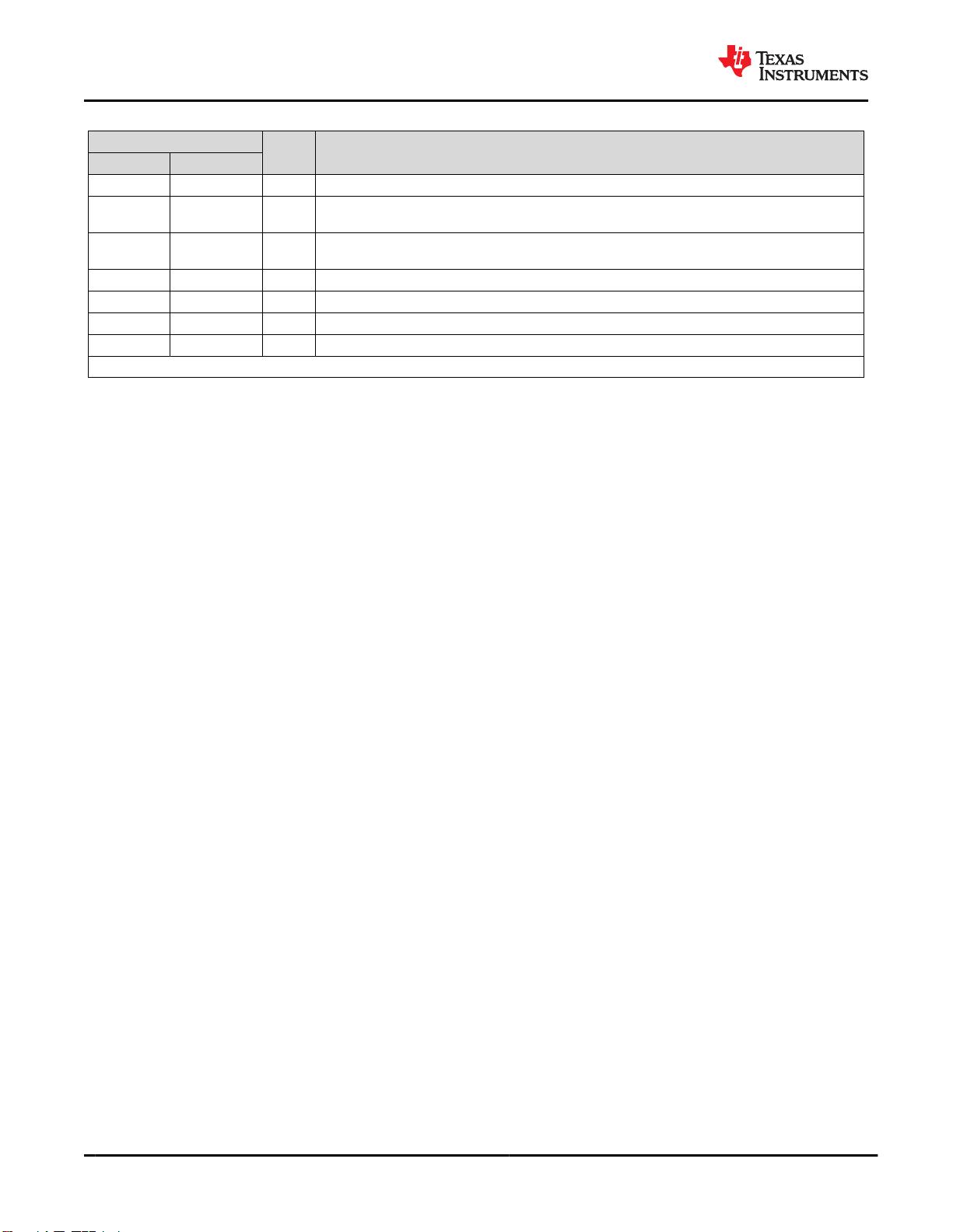
自动 PWM/PFM(AUTO 模式)运行可在降压转换器
的较宽输出电流范围内实现较高效率。
该器件包含一次性可编程 (OTP) 内存。对于给定的应
用,每个可订购器件型号都有特定的 OTP 设置。有关
每个可订购器件型号的默认 OTP 配置的详细信息,请
参见技术参考手册。
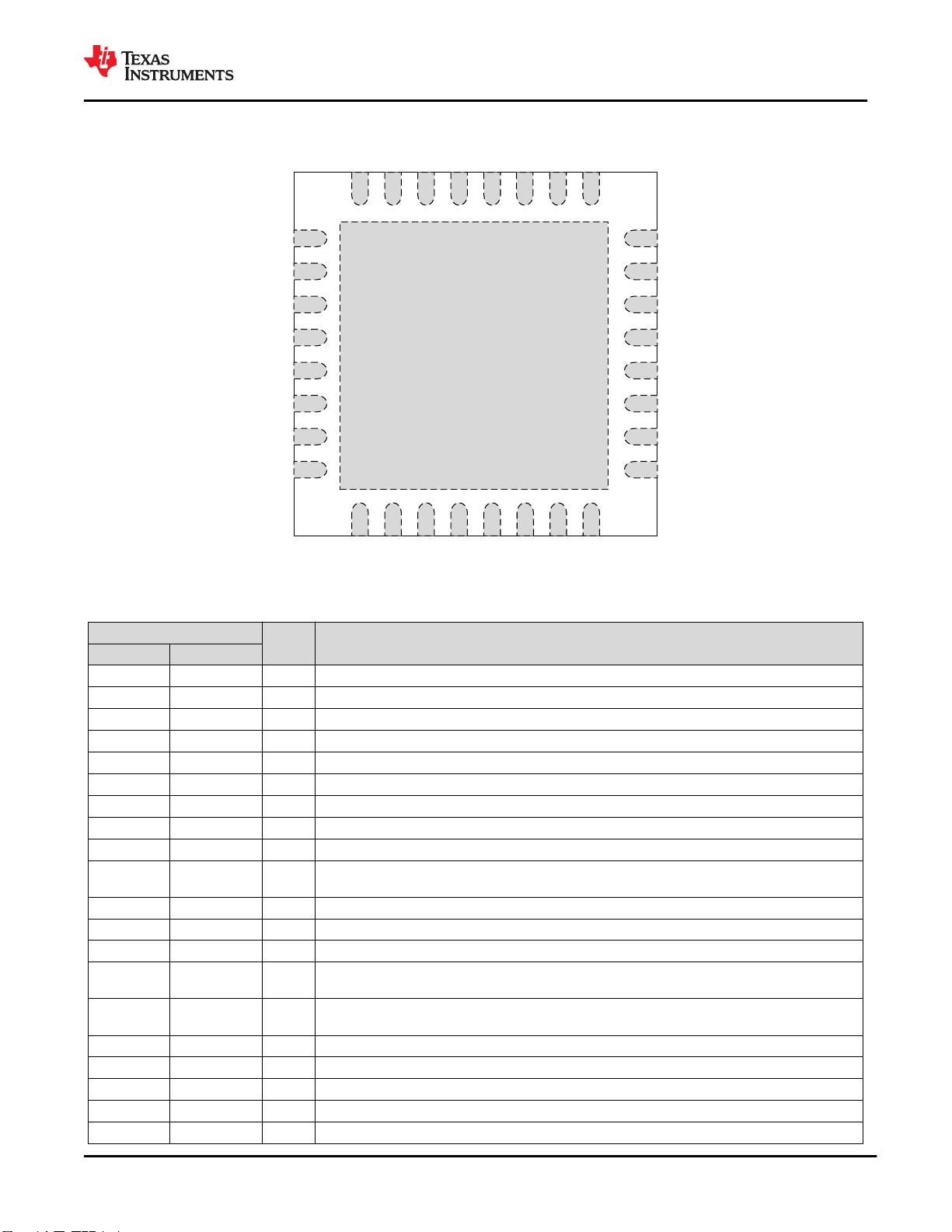
器件信息
(1)
器件型号 封装 封装尺寸(标称值)
LP87702 VQFN (32) 5.00mm × 5.00mm
(1) 如需了解所有可用封装,请参阅数据表末尾的可订购产品附
录。
Copyright © 2017, Texas Instruments Incorporated
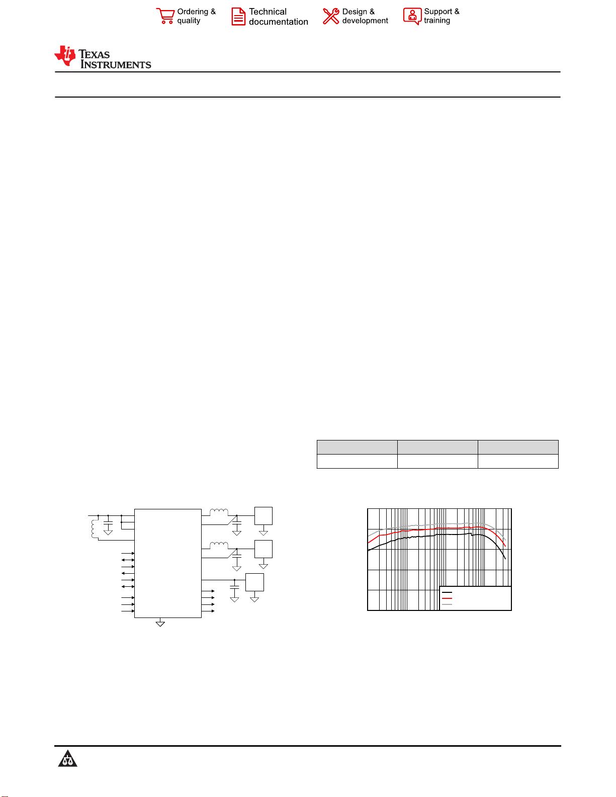
SW_B0VIN_B0
VIN_B1
VANA
VIN
FB_B0
VOUT0
LOAD
SDA (EN3)
SCL (EN2)
nINT
CLKIN (GPO2/WD_DIS)
GNDs
EN1
SW_B1
FB_B1
VOUT1
PG0
VMON1
VMON2
PG1 (GPO1)
WDI WD_RESET
SW_BST
VOUT_BST
VOUT2
LOAD
LOAD
GPO0
NRST
简化版原理图
Output Current (mA)
Efficiency (%)
1 10 100 1000 5000
50
60
70
80
90
100
Exce
VIN=3.3V, VOUT=1.2V
VIN=3.3V, VOUT=1.8V
VIN=3.3V, VOUT=2.3V
降压效率与输出电流的关系
LP87702
ZHCSNP2 – MARCH 2021
本文档旨在为方便起见,提供有关 TI 产品中文版本的信息,以确认产品的概要。有关适用的官方英文版本的最新信息,请访问
www.ti.com,其内容始终优先。TI 不保证翻译的准确性和有效性。在实际设计之前,请务必参考最新版本的英文版本。
English Data Sheet: SNVSBU3
剩余97页未读,继续阅读
资源评论


不觉明了
- 粉丝: 7489
- 资源: 5764


最新资源
- 基于微信小程序的宠物寄养平台的设计与实现+ssm-微信小程序毕业项目,适合计算机毕-设、实训项目、大作业学习.rar
- 基于微信小程序的图书馆座位预约_7kci7-微信小程序毕业项目,适合计算机毕-设、实训项目、大作业学习.zip
- 基于微信小程序的实习生管理系统bootpf-微信小程序毕业项目,适合计算机毕-设、实训项目、大作业学习.zip
- 多配送中心的路径规划问题VRP-MultiDepot 该资源使用两阶段法来解决多配送中心的问题,通过构造蚁群算法来对模型进行求解,在应用2-opt方法对最优解进行更新,程序源码使用的为Matlab
- 基于微信小程序的电影院订票选座系统ssm-微信小程序毕业项目,适合计算机毕-设、实训项目、大作业学习.rar
- 基于微信小程序的小微金融企业的设计与实现_3539r-微信小程序毕业项目,适合计算机毕-设、实训项目、大作业学习.zip
- 基于微信小程序的闲置品交易平台_1509x-微信小程序毕业项目,适合计算机毕-设、实训项目、大作业学习.zip
- 基于微信小程序的家政服务预约系统的设计与实现+php-微信小程序毕业项目,适合计算机毕-设、实训项目、大作业学习.rar
- 基于微信小程序的小区服务管理系统pf-微信小程序毕业项目,适合计算机毕-设、实训项目、大作业学习.zip
- 基于微信小程序的大学生科技竞赛管理系统的设计与实现+springboot-微信小程序毕业项目,适合计算机毕-设、实训项目、大作业学习.rar
- Python 项目实例,展示如何实现基于深度置信网络(DBN)进行多输入单输出回归预测(含完整的程序,GUI设计和代码详解)
- 基于微信小程序的校医务室健康服务系统_06pr7-微信小程序毕业项目,适合计算机毕-设、实训项目、大作业学习.zip
- 基于微信小程序的周边美食推荐系统_2axo8-微信小程序毕业项目,适合计算机毕-设、实训项目、大作业学习.zip
- 基于微信小程序的校园二手交易平台ssm-微信小程序毕业项目,适合计算机毕-设、实训项目、大作业学习.rar
- 基于微信小程序的民宿短租系统设计与实现+ssm-微信小程序毕业项目,适合计算机毕-设、实训项目、大作业学习.rar
- 基于微信小程序疫苗预约系统+ssm-微信小程序毕业项目,适合计算机毕-设、实训项目、大作业学习.rar
资源上传下载、课程学习等过程中有任何疑问或建议,欢迎提出宝贵意见哦~我们会及时处理!
点击此处反馈


