没有合适的资源?快使用搜索试试~ 我知道了~
LP5862是一款2×18 LED矩阵驱动器,具备8位模拟调光和8/16位PWM调光功能。它适用于需要精确控制和高效能LED显示的应用。这款驱动器采用LED矩阵拓扑结构,能配置1到2个扫描开关,用于36个LED点,提供18个恒流源,每个可独立控制0.1mA至50mA的电流,适用于2.7V至5.5V的工作电压范围。 该驱动器具有高精度的恒流源,设备间误差和通道间误差均控制在±5%,并具有相位移功能,确保动态响应时的功率平衡。在低功耗设计方面,当EN引脚为低电平时,待机模式下的电流消耗不超过2uA;EN引脚为高电平且CHIP_EN为0时,待机模式下电流消耗不超过10uA;在活动模式下,当通道电流为5mA时,电流消耗仅为3mA(典型值)。 LP5862提供了灵活的调光选项,包括对每个LED点的独立开/关控制、模拟调光(电流增益控制)、全局3位最大电流(MC)设置、3组7位颜色电流(CC)设置(针对红色、绿色和蓝色)。此外,还支持每个LED点的8位或16位PWM调光,确保无噪音的频率调光。它还配备了全地址SRAM,减少数据传输,同时具备单独LED点开路和短路检测功能,以及去鬼影和低亮度补偿技术。 接口方面,LP5862支持最高1MHz的I2C接口(IFS低电平时)和最高12MHz的SPI接口(IFS高电平时),满足不同速度需求。其广泛应用于键盘、鼠标、游戏外设、智能家居电器、智能音箱、有线和无线音箱、音频混音器、DJ设备、广播设备、接入设备、开关和服务器等,为电子产品的LED动画和指示功能提供高性能解决方案。此外,LP5862的恒流源特性也使其适用于光学模块应用,进一步提升系统的显示效果和用户体验。
资源推荐
资源详情
资源评论

LP5862 2 × 18 LED Matrix Driver With 8-Bit Analog and 8-/16-Bit PWM Dimming
1 Features
• LED matrix topology:
– 18 constant current sinks with 2 scan switches
for 36 LED dots
– Configurable for 1 to 2 scan switches
• Operating voltage range:
– V
CC
/V
LED
range: 2.7 V to 5.5 V
– Logic pins compatible with 1.8 V, 3.3 V, and 5 V
• 18 constant current sinks with high precision:
– 0.1 mA–50 mA per current sink when V
CC
≥ 3.3
V
– Device-to-device error: ±5%
– Channel-to-channel error: ±5%
– Phase-shift for balanced transient power
• Ultra-low power consumption:
– Shutdown mode: I
CC
≤ 2 uA when EN = Low
– Standby mode: I
CC
≤ 10 uA when EN = High
and CHIP_EN = 0 (data retained)
– Active mode: I
CC
= 3 mA (typ.) when channel
current = 5 mA
• Flexible dimming options:
– Individual ON and OFF control for each LED
dot
– Analog dimming (current gain control)
• Global 3-bit Maximum Current (MC) setting
for all LED dots
• 3 groups of 7-bit Color Current (CC) setting
for red, green, and blue
• Individual 8-bit Dot Current (DC) setting for
each LED dot
– PWM dimming with audible-noise-free
frequency
• Global 8-bit PWM dimming for all LED dots
• 3 programmable groups of 8-bit PWM
dimming for LED dot arbitrary mapping
• Individual 8-bit or 16-bit PWM dimming for
each LED dot
• Full addressable SRAM to minimize data traffic
• Individual LED dot open and short detection
• Deghosting and low brightness compensation
• Interface options:
– 1-MHz (max.) I
2
C interface when IFS = Low
– 12-MHz (max.) SPI interface when IFS = High
2 Applications
• LED animation and indication for:
– Keyboard, mouse, and gaming accessories
– Major and smart home appliances
– Smart speaker, wired and wireless speaker
– Audio mixer, DJ equipment, and broadcast
– Access equipment, switches, and servers
• Constant current sinks for optical module
3 Description
Electronic devices are becoming smarter, requiring
to use larger quantity of LEDs for animation and
indication purposes and high performance LED matrix
driver is required to improve user experience with
small solution size.
The LP586x devices are a family of high performance
LED matrix drivers. The device integrates 18 constant
current sinks with N (N = 1/2/4/6/8/11) switching
MOSFETs to support N × 18 LED dots or N × 6 RGB
LEDs. The LP5862 integrates 2 MOSFETs for up to
36 LED dots or 12 RGB LEDs.
The LP5862 supports both analog dimming and
PWM dimming methods. For analog dimming, each
LED dot can be adjusted with 256 steps. For PWM
dimming, the integrated 8-bit or 16-bit configurable
PWM generators enable smooth and audible-noise-
free dimming control. Each LED dot can also be
arbitrarily mapped into 8-bit Group PWM to achieve
dimming control together.
The LP5862 device implements full addressable
SRAM to minimize the data traffic. The ghost-
cancellation circuitry is integrated to eliminate both
upside and downside ghosting. The LP5862 also
supports LED open and short detection functions.
Both 1-MHz (maximum) I
2
C and 12-MHz (maximum)
SPI are available in LP5862.
Device Information
PART NUMBER PACKAGE
(1)
BODY SIZE (NOM)
LP5862 VQFN (32) 4 mm × 4 mm
(1) For all available packages, see the orderable addendum at
the end of the data sheet.
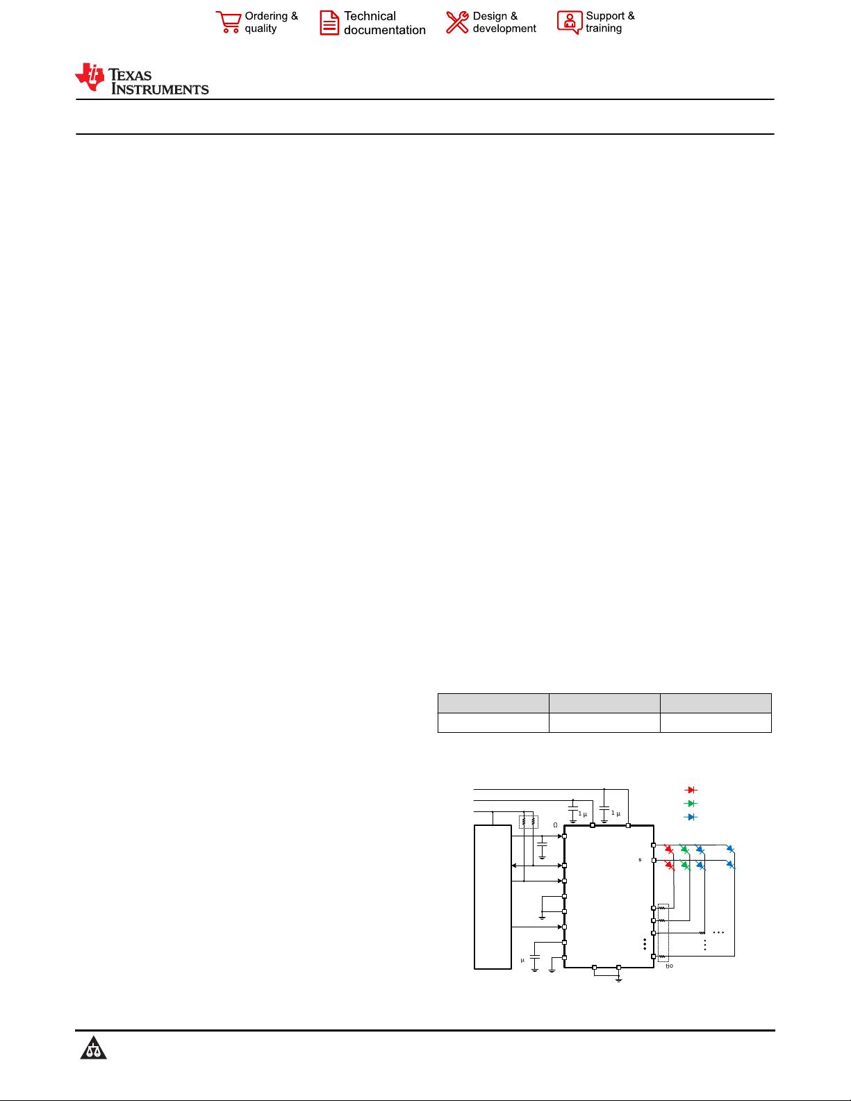
VIO_EN
SDA_MOSI
SCL_SCLK
SW0
CS17
MCU
VCC
GND
LP5862
ADDR1_MISO
VCAP
CS2
CS0
VSYNC
CS1
VLED
ADDR2_SS
IFS
V
LED
: 2.7 V to 5.5 V
V
CC
: 2.7 V to 5.5 V
C
VLED
C
VCC
C
VIO
V
IO
: 1.8 V to 5 V
R
Pullup
C
VCAP
AGND
4.7 k
1
F
1
F
1 nF
1
F
Op
onal
SW1
Red LED
Green LED
Blue LED
Simplified Schematic
LP5862
SNVSC53 – DECEMBER 2021
An IMPORTANT NOTICE at the end of this data sheet addresses availability, warranty, changes, use in safety-critical applications,
intellectual property matters and other important disclaimers. PRODUCTION DATA.

Table of Contents
1 Features............................................................................1
2 Applications..................................................................... 1
3 Description.......................................................................1
4 Revision History.............................................................. 2
5 Device Comparison......................................................... 3
6 Pin Configuration and Functions...................................4
7 Specifications.................................................................. 6
7.1 Absolute Maximum Ratings........................................ 6
7.2 ESD Ratings............................................................... 6
7.3 Recommended Operating Conditions.........................6
7.4 Thermal Information....................................................6
7.5 Electrical Characteristics.............................................7
7.6 Timing Requirements.................................................. 8
7.7 Typical Characteristics.............................................. 11
8 Detailed Description......................................................13
8.1 Overview................................................................... 13
8.2 Functional Block Diagram......................................... 13
8.3 Feature Description...................................................13
8.4 Device Functional Modes..........................................22
8.5 Programming............................................................ 23
8.6 Register Maps...........................................................26
9 Application and Implementation.................................. 31
9.1 Application Information............................................. 31
9.2 Typical Application.................................................... 31
10 Power Supply Recommendations..............................34
11 Layout........................................................................... 35
11.1 Layout Guidelines................................................... 35
11.2 Layout Example...................................................... 35
12 Device and Documentation Support..........................36
12.1 Documentation Support.......................................... 36
12.2 Receiving Notification of Documentation Updates..36
12.3 Support Resources................................................. 36
12.4 Trademarks............................................................. 36
12.5 Electrostatic Discharge Caution..............................36
12.6 Glossary..................................................................36
13 Mechanical, Packaging, and Orderable
Information.................................................................... 37
4 Revision History
NOTE: Page numbers for previous revisions may differ from page numbers in the current version.
DATE REVISION NOTES
December 2021 * Initial release
LP5862
SNVSC53 – DECEMBER 2021
www.ti.com
2 Submit Document Feedback
Copyright © 2021 Texas Instruments Incorporated
Product Folder Links: LP5862

5 Device Comparison
PART NUMBER MATERIAL LED DOT NUMBER PACKAGE
(2)
SOFTWARE
COMPATIBLE
LP5861 LP5861RSMR 18 × 1 = 18 VQFN-32
Yes
LP5862
LP5862RSMR
18 × 2 = 36
VQFN-32
LP5862DBTR TSSOP-38
LP5864
LP5864RSMR
18 × 4 = 72 VQFN-32
LP5864MRSMR
(1)
LP5866
LP5866RKPR
18 × 6 = 108
VQFN-40
LP5866DBTR
TSSOP-38
LP5866MDBTR
(1)
LP5868 LP5868RKPR 18 × 8 = 144 VQFN-40
LP5860
LP5862RKPR
18 × 11 = 198 VQFN-40
LP5862MRKPR
(1)
(1) Extended Temperature devices, supporting –55°C to approximately 125°C operating ambient temperature.
(2) The same packages are hardware compatible.
www.ti.com
LP5862
SNVSC53 – DECEMBER 2021
Copyright © 2021 Texas Instruments Incorporated
Submit Document Feedback
3
Product Folder Links: LP5862

6 Pin Configuration and Functions
1
2
3
4
5
6
7
8
9
10
11
12
13
14
15
16
GND
24
23
22
21
20
19
18
17
32
31
30
29
28
27
26
25
VCC
CS8
SW0
SW0
SW1
VLED
CS9
CS10
CS11
CS12
CS13
CS14
CS15
CS16
CS17
CS6
CS5
CS4
CS3
CS2
CS1
VCAP
CS0
VIO_EN
ADDR1_SS
ADDR0_MISO
VSYNC
SDA_MOSI
SCL_SCLK
IFS
CS7
SW1
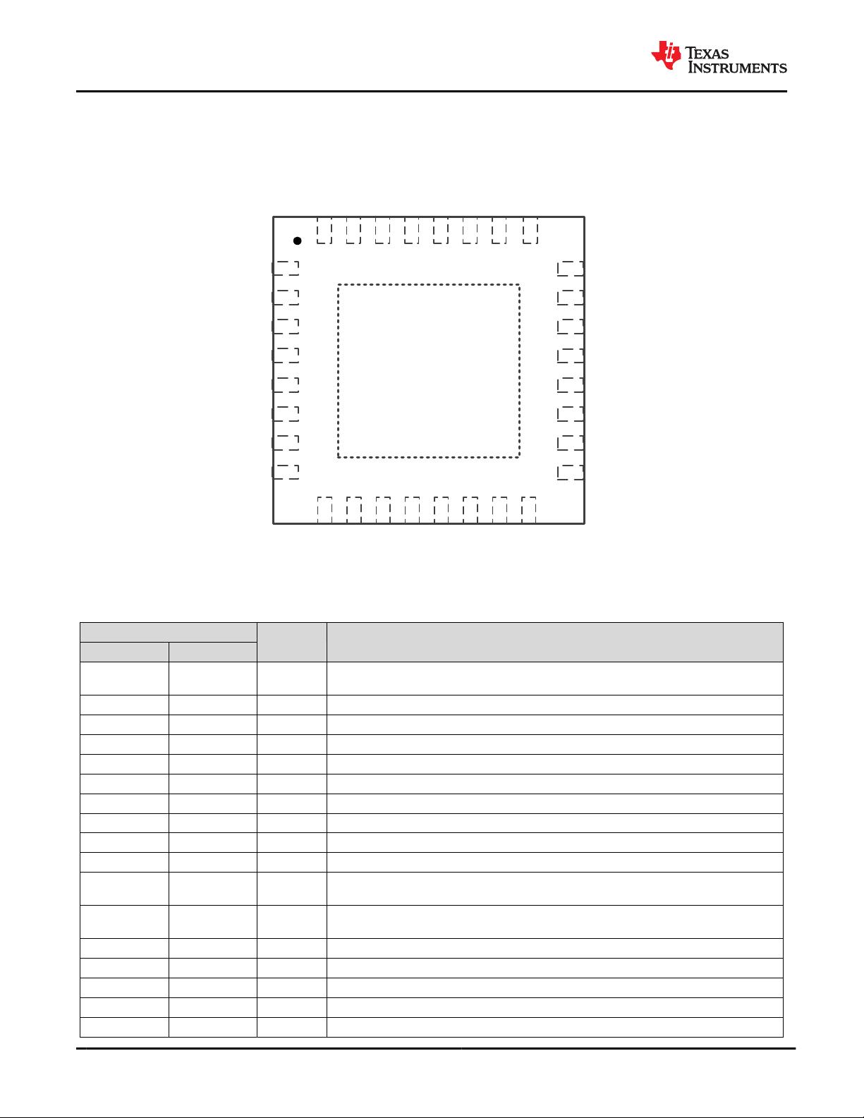
Figure 6-1. LP5862 RKP Package 40-Pin VQFN With Exposed Thermal Pad Top View
Table 6-1. Pin Functions
PIN
I/O DESCRIPTION
NO. NAME
1 VCC
Power
Power supply for device. A 1-μF capacitor must be connected between this pin with GND
and be placed as close to the device as possible.
2 CS0 O Current sink 0. If not used, this pin must be left floating.
3 CS1 O Current sink 1. If not used, this pin must be left floating.
4 CS2 O Current sink 2. If not used, this pin must be left floating.
5 CS3 O Current sink 3. If not used, this pin must be left floating.
6 CS4 O Current sink 4. If not used, this pin must be left floating.
7 CS5 O Current sink 5. If not used, this pin must be left floating.
8 CS6 O Current sink 6. If not used, this pin must be left floating.
9 CS7 O Current sink 7. If not used, this pin must be left floating.
10 CS8 O Current sink 8. If not used, this pin must be left floating.
11/12 SW0 O
High-side PMOS switch output 0. Both 2 pins must be tied together. If not used, this pin
must be left floating.
13/14 SW1 O
High-side PMOS switch output 1. Both 2 pins must be tied together. If not used, this pin
must be left floating.
15 VLED Power Power input for high-side switches
16 CS9 O Current sink 9. If not used, this pin must be left floating.
17 CS10 O Current sink 10. If not used, this pin must be left floating.
18 CS11 O Current sink 11. If not used, this pin must be left floating.
19 CS12 O Current sink 12. If not used, this pin must be left floating.
LP5862
SNVSC53 – DECEMBER 2021
www.ti.com
4 Submit Document Feedback
Copyright © 2021 Texas Instruments Incorporated
Product Folder Links: LP5862

Table 6-1. Pin Functions (continued)
PIN
I/O DESCRIPTION
NO. NAME
20 CS13 O Current sink 13. If not used, this pin must be left floating.
21 CS14 O Current sink 14. If not used, this pin must be left floating.
22 CS15 O Current sink 15. If not used, this pin must be left floating.
23 CS16 O Current sink 16. If not used, this pin must be left floating.
24 CS17 O Current sink 17. If not used, this pin must be left floating.
25 VCAP O
Internal LDO output. An 1-μF capacitor must be connected between this pin with GND.
Place the capacitor as close to the device as possible.
26 IFS I
Interface type select. I
2
C is selected when IFS is low. SPI is selected when IFS is high. A
resistor must be connected between VIO and this pin.
27 VSYNC I External synchronize signal for display mode 2 and mode 3
28 SCL_SCLK I I
2
C clock input or SPI clock input. Pull up to VIO when configured as I
2
C.
29 SDA_MOSI I/O I
2
C data input or SPI leader output follower input. Pull up to VIO when configured as I
2
C.
30 ADDR0_MISO I/O I
2
C address select 0 or SPI leader input follower output
31 ADDR1_SS I I
2
C address select 1 or SPI follower select
32 VIO_EN Power,I
Power supply for digital circuits and chip enable. A 1-nF capacitor must be connected
between this pin with GND and be placed as close to the device as possible.
Exposed
Thermal Pad
GND Ground Common ground plane
www.ti.com
LP5862
SNVSC53 – DECEMBER 2021
Copyright © 2021 Texas Instruments Incorporated
Submit Document Feedback
5
Product Folder Links: LP5862
剩余42页未读,继续阅读
资源评论

不觉明了
- 粉丝: 4967
- 资源: 5759
上传资源 快速赚钱
 我的内容管理
展开
 我的资源
快来上传第一个资源
 我的收益 登录查看自己的收益
 我的积分
登录查看自己的积分
 我的C币
登录后查看C币余额
 我的收藏
我的收藏  我的下载
我的下载  下载帮助
下载帮助

 前往需求广场,查看用户热搜
最新资源
资源上传下载、课程学习等过程中有任何疑问或建议,欢迎提出宝贵意见哦~我们会及时处理!
点击此处反馈


安全验证
文档复制为VIP权益,开通VIP直接复制
 信息提交成功