ddr3中文数据手册Micron -MT4C4001J
需积分: 10 89 浏览量
2022-11-18
22:34:49
上传
评论 5
收藏 314KB PDF 举报

DRAM
MT4C4001J
Austin Semiconductor, Inc.
MT4C4001J
Rev. 1.0 9/01
Austin Semiconductor, Inc. reserves the right to change products or specifications without notice.
1
For more products and information
please visit our web site at
www.austinsemiconductor.com
AVAILABLE AS MILITARY
SPECIFICATIONS
• SMD 5962-90847
• MIL-STD-883
1 MEG x 4 DRAM
Fast Page Mode DRAM
FEATURES
• Industry standard x4 pinout, timing, functions, and
packages
• High-performance, CMOS silicon-gate process
• Single +5V±10% power supply
• Low-power, 2.5mW standby; 300mW active, typical
• All inputs, outputs, and clocks are fully TTL and CMOS
compatible
• 1,024-cycle refresh distributed across 16ms
• Refresh modes: RAS\-ONLY, CAS\-BEFORE-RAS\
(CBR), and HIDDEN
• FAST PAGE MODE access cycle
• CBR with WE\ a HIGH (JEDEC test mode capable via
WCBR)
OPTIONS MARKING
• Timing
70ns access -7
80ns access -8
100ns access -10
120ns access -12
• Packages
Ceramic DIP (300 mil) CN No. 103
Ceramic DIP (400 mil) C No. 104
Ceramic LCC* ECN No. 202
Ceramic ZIP CZ No. 400
Ceramic SOJ ECJ No. 504
Ceramic Gull Wing ECG No. 600
*NOTE: If solder-dip and lead-attach is desired on LCC
packages, lead-attach must be done prior to the solder-
dip operation.
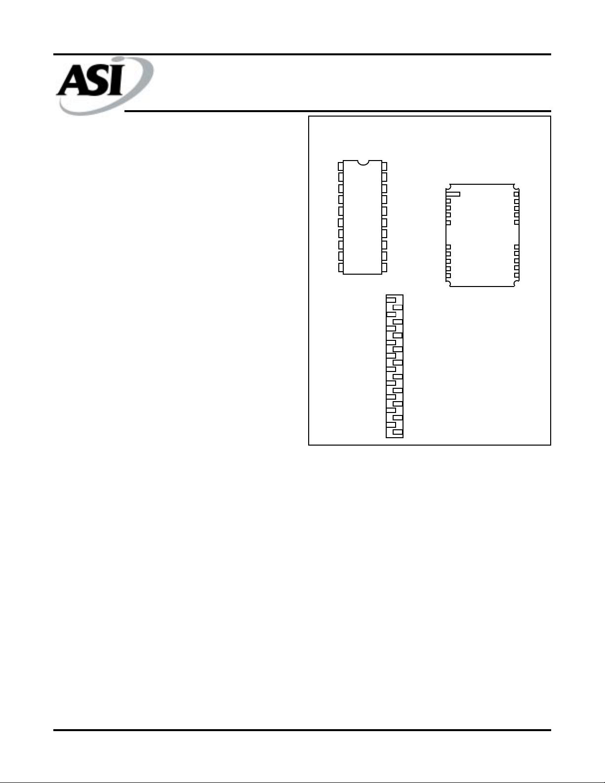
PIN ASSIGNMENT
(Top View)
20-Pin DIP (C, CN)
1
2
3
4
5
6
7
8
9
10
20
19
18
17
16
15
14
13
12
11
DQ1
DQ2
WE\
RAS\
A9
A0
A1
A2
A3
Vcc
Vss
DQ4
DQ3
CAS\
OE\
A8
A7
A6
A5
A4
1
2
3
4
5
9
10
11
12
13
26
25
24
23
22
18
17
16
15
14
DQ1
DQ2
WE\
RAS\
A9
A0
A1
A2
A3
Vcc
Vss
DQ4
DQ3
CAS\
OE\
A8
A7
A6
A5
A4
20-Pin SOJ (ECJ),
20-Pin LCC (ECN), &
20-Pin Gull Wing (ECG)
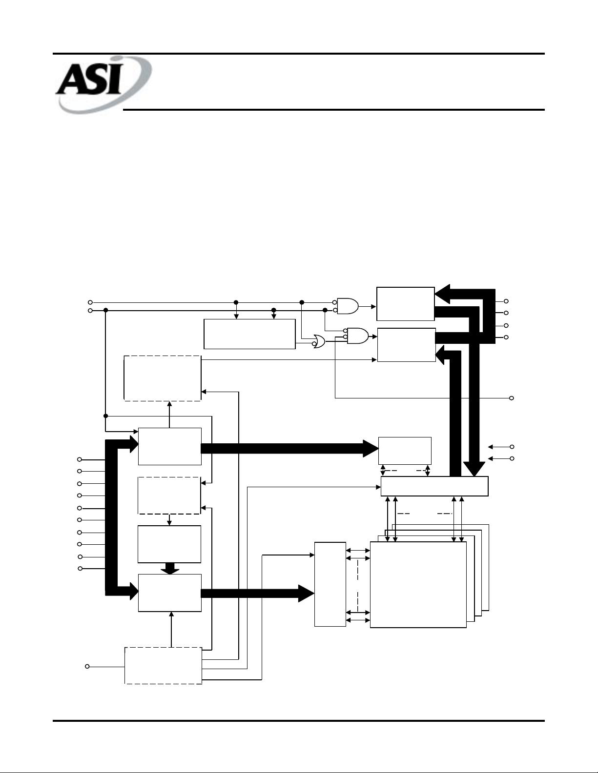
GENERAL DESCRIPTION
The MT4C4001J is a randomly accessed solid-state
memory containing 4,194,304 bits organized in a x4
configuration. During READ or WRITE cycles each bit is
uniquely addressed through the 20 address bits which are
entered 10 bits (A0-A9) at a time. RAS\ is used to latch the
first 10 bits and CAS\ the later 10 bits. A READ or WRITE
cycle is selected with the WE\ input. A logic HIGH on WE\
dictates READ mode while a logic LOW on WE\ dictates
WRITE mode. During a WRITE cycle, data-in (D) is latched
by the falling edge of WE\ or CAS\, whichever occurs last. If
WE\ goes LOW prior to CAS\ going LOW, the output pin(s)
remain open (High-Z) until the next CAS\ cycle. If WE\ goes
LOW after data reaches the output pin(s), Qs are activated and
retain the selected cell data as long as CAS\ remains low
(regardless of WE\ or RAS\). This LATE WE\ pulse results in
a READ-WRITE cycle. The four data inputs and four data
outputs are routed through four pins using common I/O and
pin direction is controlled by WE\ and OE\. FAST-PAGE-
MODE operations allow faster data operations (READ,
WRITE, or READ-MODIFY-WRITE) within a row address
(A0-A9) defined page boundary. The FAST PAGE MODE
(continued)
20-Pin DIP (CZ)
OE\ 1
DQ3 3
Vss 5
DQ2 7
RAS\ 9
A0 11
A2 13
Vcc 15
A5 17
A7 19
2 CAS\
4 DQ4
6 DQ1
8 WE\
10 A9
12 A1
14 A3
16 A4
18 A6
20 A8

剩余20页未读,继续阅读


评论0
最新资源