TI-LM5070.pdf
需积分: 10 152 浏览量
2022-11-16
23:24:53
上传
评论 5
收藏 1.08MB PDF 举报

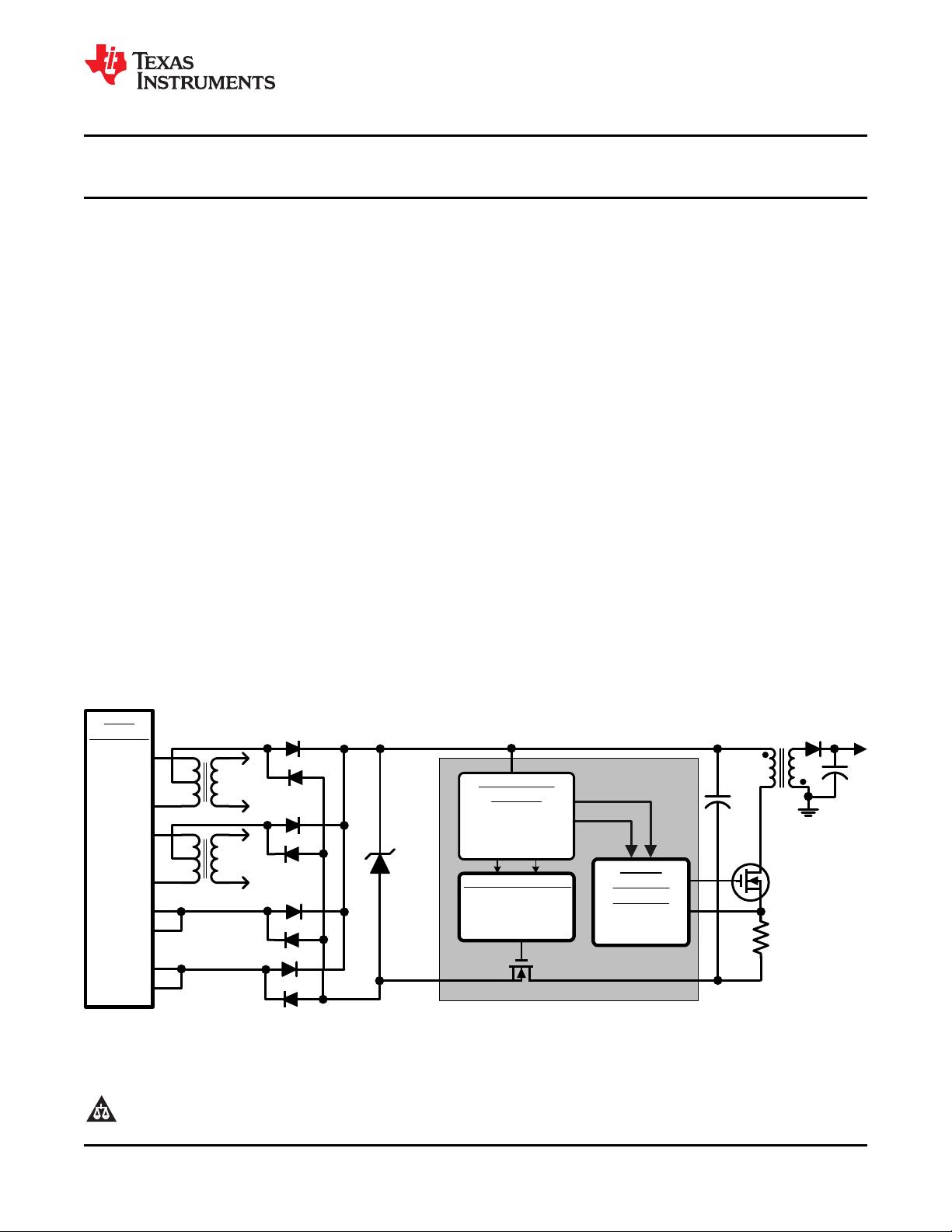
RJ45
Connector
TX+ (1)
TX- (2)
RX+ (3)
RX- (6)
(4)
(7)
(5)
(8)
To PHY
To PHY
Hot Plug Controller
In-rush and Fault
Current Limiting
DC-DC
Converter
Controller
Current Mode
IEEE 802.3af
Interface
UVLO
Signature Detection
Classification
LM5070
VDC
LM5070
www.ti.com
SNVS308G –OCTOBER 2004–REVISED APRIL 2013
LM5070 Integrated Power Over Ethernet PD Interface and PWM Controller
Check for Samples: LM5070
1
FEATURES
DESCRIPTION
The LM5070 power interface port and pulse width
2
• Fully Compliant 802.3af Power Interface Port
modulation (PWM) controller provides a complete
• 80V, 1Ω, 400 mA Internal MOSFET
integrated solution for Powered Devices (PD) that
• Programmable Inrush Current Limit
connect into Power over Ethernet (PoE) systems. The
LM5070 integrates an 80V, 400mA line connection
• Detection Resistor Disconnect Function
switch and associated control for a fully IEEE 802.3af
• Programmable Classification Current
compliant interface with a full featured current mode
• Programmable Under-voltage Lockout with
pulse width modulator dc-dc converter. All power
Programmable Hysteresis
sequencing requirements between the controller
interface and switch mode power supply (SMPS) are
• Thermal Shutdown Protection
integrated into the IC. Two options are available
• Current Mode Pulse Width Modulator
providing either an 80% maximum duty cycle limit
• Supports Both Isolated and Non-Isolated
with slope compensation (on the –80 suffix) device or
Applications
a 50% maximum duty cycle limit and no slope
compensation on the (–50 suffix) device.
• Error Amplifier and Reference for Non-Isolated
Applications
PACKAGES
• Programmable Oscillator Frequency
• TSSOP-16
• Programmable Soft-Start
• WSON-16 (5 mm x 5 mm)
• 80% Maximum Duty Cycle Limiter, Slope
Compensation (-80 device)
• 50% Maximum Duty Cycle Limiter, No Slope
Compensation (-50 device)
• 800 mA Peak Gate Driver
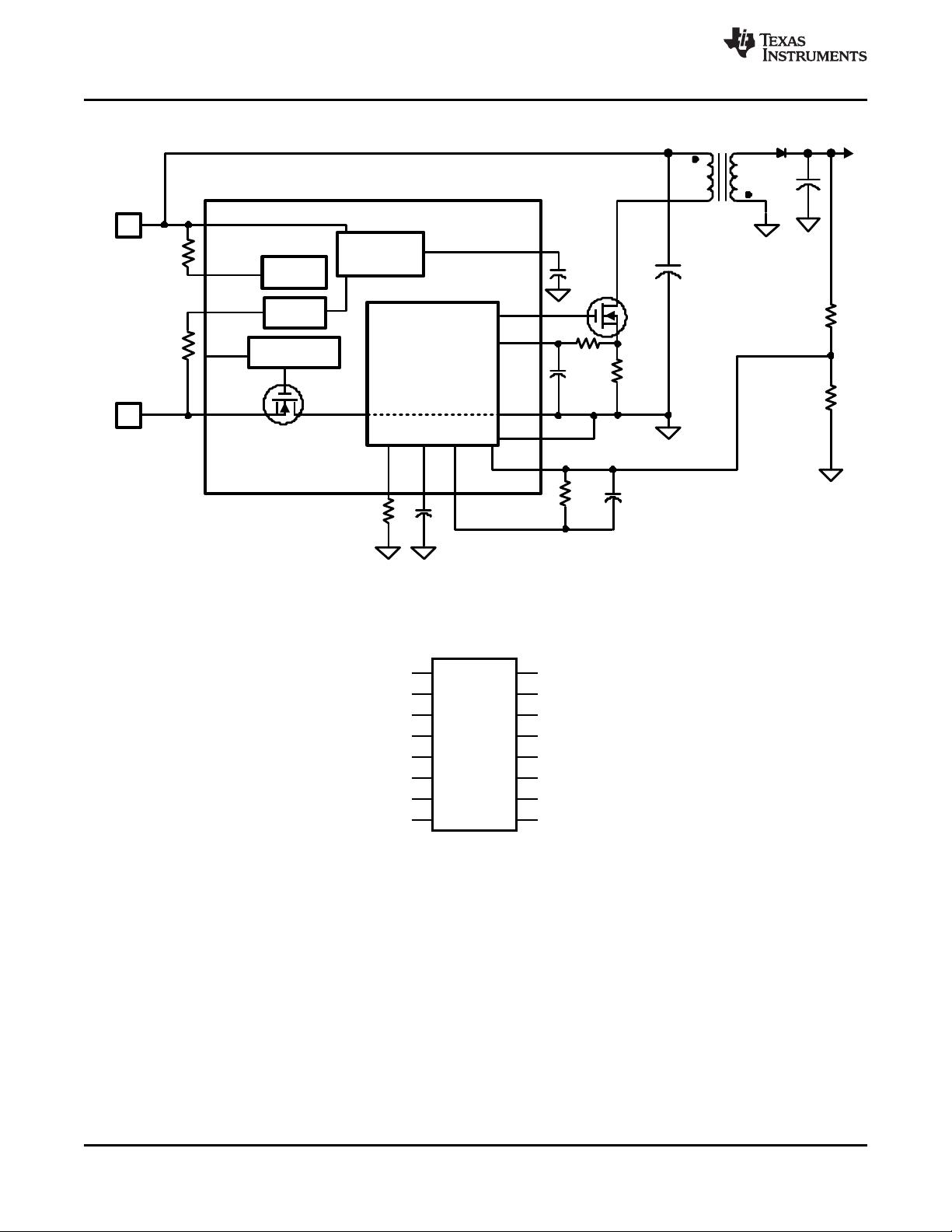
Block Diagrams
1
Please be aware that an important notice concerning availability, standard warranty, and use in critical applications of
Texas Instruments semiconductor products and disclaimers thereto appears at the end of this data sheet.
2All trademarks are the property of their respective owners.
PRODUCTION DATA information is current as of publication date.
Copyright © 2004–2013, Texas Instruments Incorporated
Products conform to specifications per the terms of the Texas
Instruments standard warranty. Production processing does not
necessarily include testing of all parameters.
剩余23页未读,继续阅读


评论0
最新资源