没有合适的资源?快使用搜索试试~ 我知道了~
TI-LM96163.pdf
需积分: 5 0 下载量 117 浏览量
2023-04-22
16:11:06
上传
评论
收藏 1.42MB PDF 举报
温馨提示
![preview](https://dl-preview.csdnimg.cn/87715820/0001-8e4d29336da449196d2f7a5764764277_thumbnail.jpeg)
![preview-icon](https://csdnimg.cn/release/downloadcmsfe/public/img/scale.ab9e0183.png)
试读
50页
TI-LM96163.pdf
资源推荐
资源详情
资源评论
![](https://csdnimg.cn/release/download_crawler_static/87715820/bg1.jpg)
LM96163
www.ti.com
SNAS433D –JUNE 2008–REVISED MAY 2013
LM96163 Remote Diode Digital Temperature Sensor with Integrated Fan Control and
TruTherm
®
BJT Transistor Beta Compensation Technology
Check for Samples: LM96163
1
FEATURES
DESCRIPTION
The LM96163 has remote and local temperature
2
• TruTherm BJT Beta Compensation Technology
sensors with integrated fan control that includes
Supports 45nm, 65nm and 90nm Processor
TruTherm BJT transistor beta compensation
Remote Diodes
technology for remote diode sensing. The LM96163
• Factory Trimmed for Intel® 45 nm Processor
accurately measures: (1) its own temperature and (2)
Thermal Diodes
the temperature of a diode-connected transistor, such
as a 2N3904, or a thermal diode commonly found on
• Accurately Senses Diode-Connected 2N3904
Computer Processors, Graphics Processor Units
Transistors or Thermal Diodes On-board Large
(GPU) and other ASIC's. The LM96163 has an offset
Processors or ASIC's
register to correct for errors caused by different non-
• Accurately Senses its Own Temperature
ideality factors of other thermal diodes.
• Integrated PWM Fan Speed Control Output
The LM96163 also features an integrated, pulse-
Supports High Resolution at 22.5kHz
width-modulated (PWM), open-drain fan control
Frequency for 4-pin Fans
output. Fan speed depends on a combination of the
• Acoustic Fan Noise Reduction with User-
remote temperature reading, the lookup table and
Programmable 12-Step Lookup Table
register settings. The 12-step Lookup Table (LUT)
enables the user to program a non-linear fan speed
• LUT Transition Fine Resolution Smoothing
vs. temperature transfer function often used to quiet
Function
acoustic fan noise. In addition a fully programmable
• Tachometer Input for Measuring Fan RPM
ramping function has been added to allow smooth
• Smart-Tach Modes for Measuring RPM of Fans transitions between LUT setpoints.
with Pulse-Width-Modulated Power as Shown
Table 1. Key Specifications
in Typical Application
■ Remote Temp Accuracy (includes quantization error)
• ALERT Output for Processor Event
LM96163 Temp DiodeTemp Max Error
Notification
+25 to +85°C +50 to +105°C ±0.75°C
• TCRIT Output for Critical Temperature System
+25 to +85°C +40 to +125°C ±1.5°C
Shutdown
-40 to +25°C +25 to 125°C ±3.0°C
• Offset Register Can Adjust for a Variety of
■ Local Temp Accuracy (includes quantization error)
Thermal Diodes
LM96163 Temp 25°C to 125°C ±3.0°C (max)
• 10-Bit Plus Sign and 11-Bit Unsigned Formats,
■ Supply Voltage +3.0 V to +3.6 V
with 1/8°C Resolution
■ Supply Current (0.8Hz Conversion) 456 µA (typ)
• Extended Resolution to 1/32°C when Digital
Filter Enabled
• Resolves Remote Diode Temperatures up to
255.875°C
• SMBus 2.0 Compatible Interface, with
TIMEOUT and ARA
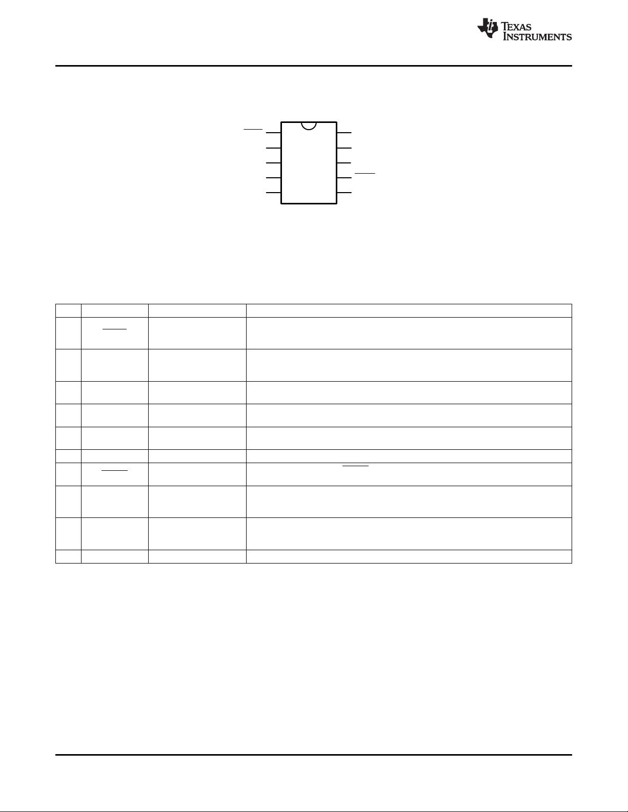
• 10-Pin SON Package
APPLICATIONS
• Processor Thermal Management
• Electronic Test and Office Equipment
• Industrial Controls
1
Please be aware that an important notice concerning availability, standard warranty, and use in critical applications of
Texas Instruments semiconductor products and disclaimers thereto appears at the end of this data sheet.
2All trademarks are the property of their respective owners.
PRODUCTION DATA information is current as of publication date.
Copyright © 2008–2013, Texas Instruments Incorporated
Products conform to specifications per the terms of the Texas
Instruments standard warranty. Production processing does not
necessarily include testing of all parameters.
![](https://csdnimg.cn/release/download_crawler_static/87715820/bg2.jpg)
LM96163
2
3
4
5
6
7
8
9
VDD
D+
D-
PWM
SMBDAT
TACH
ALERT
GND
1
10
TCRIT
SMBCLK
LM96163
SNAS433D –JUNE 2008–REVISED MAY 2013
www.ti.com
Connection Diagrams
Figure 1. 10-Pin SON (TopView)
See DSC0010A Package
Pin Descriptions
Pin Name Input/Output Function and Connection
Open-Drain Digital Output. Connect to system shutdown. Pin activates when
Open-Drain
1 TCRIT temperature conversion value exceeds programmed limit. Several power-on-default
Digital Output
limit values are available.
Connect to a low-noise +3.3 ± 0.3 V
DC
power supply, and bypass to GND with a 0.1 µF
2 V
DD
Power Supply Input ceramic capacitor in parallel with a 100 pF ceramic capacitor. A bulk capacitance of
10 µF needs to be in the vicinity of the LM96163's V
DD
pin.
Connect to the anode (positive side) of the remote diode. A 100pF capacitor can be
3 D+ Analog Input
connected between pins 3 and 4.
Connect to the cathode (negative side) of the remote diode. A 100pF capacitor can be
4 D− Analog Input
connected between pins 3 and 4.
Open-Drain Open-Drain Digital Output. Connect to fan drive circuitry. The power-on default for this
5 PWM
Digital Output pin is low (pin 4 pulled to ground).
6 GND Ground This is the analog and digital ground return.
Open-Drain This pin is an open-drain ALERT output.
7 ALERT
Digital Output
Tachometer input for measuring fan speed. Note the TACH input is disabled upon
8 TACH Digital Input power-up and needs to be enabled for use by setting TCHEN bit 2 of Configuration
Register 03h.
Digital Input/
9 SMBDAT Open-Drain Digital This is the bidirectional SMBus data line.
Output
10 SMBCLK Digital Input Digital Input. This is the SMBus clock input.
2 Submit Documentation Feedback Copyright © 2008–2013, Texas Instruments Incorporated
Product Folder Links: LM96163
![](https://csdnimg.cn/release/download_crawler_static/87715820/bg3.jpg)
100 pF
+3.3V
PWM Output
to Fan
To SMBus
interface
control
circuitry
Remote diode-
connected transistor
inside of a Processor
on 45 nm or 65 nm
process
OPTIONAL
Capacitor
is close to
pins 3 and 4
+3.3V
1.2k
Tach. input
from Fan
Fan voltage
+12 or +5 VDC
10k
13k
1k
Tach In
0.1
100 pF
10 PF
These two capacitors
are close to Pin 2
4-Pin DC Brushless
Fan Module with
Tachometer Output
and PWM Input
Fan V+
+3.3V
1.2k
1.2k
LM96163
6
7
8
9
VDD
D+
D-
PWM
SMBDAT
TACH
ALERT
GND
10
SMBCLK
TCRIT
2
3
4
5
1
1.2k
1.2k
+3.3V
To Processor Power
Supply Shutdown
TruTherm
or
Traditional
Diode
Bias and
Control
Internal Diode
LM96163-LLP10
D+
D-
2 - Wire
Serial
Interface
SMBDAT
SMBCLK
Temp Reading,
Temp Limit,
Hysteresis, and
Temp Sensor
Filter Registers
Status and Status Mask Registers and Logic
Comparators
PWM Fan Control
Registers
PWM Fan
Control
PWM
'6 ADC
IIR
Filter
Analog
Filter
ALERT
TACH
Tachometer
Detection
TCRIT
LM96163
www.ti.com
SNAS433D –JUNE 2008–REVISED MAY 2013
Simplified Block Diagram
Typical Application
Copyright © 2008–2013, Texas Instruments Incorporated Submit Documentation Feedback 3
Product Folder Links: LM96163
![](https://csdnimg.cn/release/download_crawler_static/87715820/bg4.jpg)
LM96163
SNAS433D –JUNE 2008–REVISED MAY 2013
www.ti.com
These devices have limited built-in ESD protection. The leads should be shorted together or the device placed in conductive foam
during storage or handling to prevent electrostatic damage to the MOS gates.
Absolute Maximum Ratings
(1)(2)(3)
Supply Voltage, V
DD
−0.3 V to 6.0 V
Voltage on SMBDAT, SMBCLK,ALERT, TCRIT, TACH, PWM Pins −0.5 V to 6.0 V
Voltage on Other Pins −0.3 V to (V
DD
+ 0. 3 V)
Input Current, D− Pin
(4)
±1 mA
Input Current at All Other Pins
(4)
5 mA
Package Input Current
(4)
30 mA
SMBDAT, ALERT, PWM pins
Output Sink Current 10 mA
Package Power Dissipation See
(5)
Junction Temperature 125°C
Storage Temperature −65°C to +150°C
Human Body Model 2500 V
ESD Susceptibility
(6)
Machine Model 250 V
Charged Device Model 1000 V
(1) All voltages are measured with respect to GND, unless otherwise noted.
(2) Absolute Maximum Ratings indicate limits beyond which damage to the device may occur. Operating Ratings indicate conditions for
which the device is functional, but do not guarantee performance limits. For guaranteed specifications and test conditions, see the
Electrical Characteristics. The guaranteed specifications apply only for the test conditions listed. Some performance characteristics may
degrade when the device is not operated under the listed test conditions.
(3) If Military/Aerospace specified devices are required, please contact the TI Sales Office/Distributors for availability and specifications.
(4) When the input voltage (V
IN
) at any pin exceeds the power supplies (V
IN
< GND or V
IN
> V+), the current at that pin should be limited to
5 mA. Parasitic components and/or ESD protection circuitry are shown below for the LM96163's pins. Care should be taken not to
forward bias the parasitic diode, D2, present on pins D+ and D−. Doing so by more than 50 mV may corrupt temperature
measurements.
(5) Thermal resistance junction to ambient when attached to a 2 layer 4"x3" printed circuit board with copper thickness of 2oz. as described
in JEDEC specification EIA/JESD51-3 is 137°C/W. Thermal resistance junction to ambient when attached to a 4 layer 4"x3" printed
circuit board with copper thickness 2oz./1oz./1oz/2oz. and 4 thermal vias as described in JEDEC specification EIA/JESD51-7 is
40.3°C/W.
(6) Human body model, 100 pF discharged through a 1.5 kΩ resistor. Machine model, 200 pF discharged directly into each pin. Charged
Device Model (CDM) simulates a pin slowly acquiring charge (such as from a device sliding down the feeder in an automated
assembler) then rapidly being discharged.
Operating Ratings
(1)(2)(3)(4)
Specified Temperature Range (T
MIN
≤ T
A
≤ T
MAX
) LM96163CISD –40°C ≤ T
A
≤ +85°C
Remote Diode Temperature Range -40°C ≤ T
D
≤ +140°C
Supply Voltage Range (V
DD
) +3.0 V to +3.6 V
(1) Absolute Maximum Ratings indicate limits beyond which damage to the device may occur. Operating Ratings indicate conditions for
which the device is functional, but do not guarantee performance limits. For guaranteed specifications and test conditions, see the
Electrical Characteristics. The guaranteed specifications apply only for the test conditions listed. Some performance characteristics may
degrade when the device is not operated under the listed test conditions.
(2) All voltages are measured with respect to GND, unless otherwise noted.
(3) Soldering process must comply with Reflow Temperature Profile specifications. Refer to www.ti.com/packaging
(4) Reflow temperature profiles are different for packages containing lead (Pb) than for those that do not.
4 Submit Documentation Feedback Copyright © 2008–2013, Texas Instruments Incorporated
Product Folder Links: LM96163
![](https://csdnimg.cn/release/download_crawler_static/87715820/bg5.jpg)
LM96163
www.ti.com
SNAS433D –JUNE 2008–REVISED MAY 2013
DC Electrical Characteristics
TEMPERATURE-TO-DIGITAL CONVERTER CHARACTERISTICS
The following specifications apply for V
DD
= 3.0 VDC to 3.6 VDC, and all analog source impedance R
S
= 50Ω unless
otherwise specified in the conditions. Boldface limits apply for T
A
= T
J
= T
MIN
to T
MAX
; all other limits T
A
= +25°C; unless
otherwise noted. T
D
is the junction temperature of the remote thermal diode. T
J
is the junction temperature of the LM96163.
Units
Parameter Conditions Typical
(1)
Limits
(2)
(Limits)
Temperature Error Using the Remote T
D
= +50°C to +105°C
Thermal Diode of an Intel Processor on T
A
= +25°C to +85°C T
D
= Remote Diode ±0.75 °C (max)
45nm.
(3)
Junction Temperature
T
A
= +25°C to +85°C T
D
= +40°C to +125°C ±1.5 °C (max)
T
A
= -40°C to +25°C T
D
= +25°C to +125°C ±3.0 °C (max)
Temperature Error Using the Local Diode. T
A
= +25°C to +125°C ±1 ±3 °C (max)
See
(4)
&
(5)
for the thermal resistance to be
T
A
= -40°C to +25°C
±6 °C (max)
used in the self-heating calculation.
11 Bits
Remote Diode Resolution
0.125 °C
8 Bits
Local Diode Resolution
1 °C
Conversion Time, All Temperature Channels Fastest Setting 38.3 41.1 ms (max)
D− Source Voltage 0.4 V
225 µA (max)
(V
D+
− V
D−
) = +0.65 V; High Current 172
Diode Source Current 100 µA (min)
Low Current 10.75 µA
Diode Source Current Ratio 16
(1) “Typicals” are at T
A
= 25°C and represent most likely parametric norm. They are to be used as general reference values not for critical
design calculations.
(2) Limits are guaranteed to National's AOQL (Average Outgoing Quality Level).
(3) The accuracy of the LM96163 is guaranteed when using a typical thermal diode of an Intel processor on a 45 nm process, as selected
in the Remote Diode Model Select register. See Typical Performance Characteristics for performance with Intel processor on 65 nm or
90 nm process.
(4) Local temperature accuracy does not include the effects of self-heating. The rise in temperature due to self-heating is the product of the
internal power dissipation of the LM96163 and the thermal resistance.
(5) Thermal resistance junction to ambient when attached to a 2 layer 4"x3" printed circuit board with copper thickness of 2oz. as described
in JEDEC specification EIA/JESD51-3 is 137°C/W. Thermal resistance junction to ambient when attached to a 4 layer 4"x3" printed
circuit board with copper thickness 2oz./1oz./1oz/2oz. and 4 thermal vias as described in JEDEC specification EIA/JESD51-7 is
40.3°C/W.
Operating Electrical Characteristics
Symbol Parameter Conditions Typ
(1)
Limits
(2)
Units
2.8 V (max)
V
POR
Power-On-Reset Threshold Voltage
1.6 V (min)
SMBus Inactive, 13 Hz
1.1 1.6 mA (max)
Conversion Rate
I
S
Supply Current
(3)
SMBus Inactive, 0.8 Hz
456 825 µA (max)
Conversion Rate
STANDBY Mode 416 700 µA (max)
(1) “Typicals” are at T
A
= 25°C and represent most likely parametric norm. They are to be used as general reference values not for critical
design calculations.
(2) Limits are guaranteed to National's AOQL (Average Outgoing Quality Level).
(3) The supply current will not increase substantially with an SMBus transaction.
Copyright © 2008–2013, Texas Instruments Incorporated Submit Documentation Feedback 5
Product Folder Links: LM96163
剩余49页未读,继续阅读
资源评论
![avatar-default](https://csdnimg.cn/release/downloadcmsfe/public/img/lazyLogo2.1882d7f4.png)
![avatar](https://profile-avatar.csdnimg.cn/default.jpg!1)
2301_76396056
- 粉丝: 1
- 资源: 21
上传资源 快速赚钱
我的内容管理 展开
我的资源 快来上传第一个资源
我的收益
登录查看自己的收益我的积分 登录查看自己的积分
我的C币 登录后查看C币余额
我的收藏
我的下载
下载帮助
![voice](https://csdnimg.cn/release/downloadcmsfe/public/img/voice.245cc511.png)
![center-task](https://csdnimg.cn/release/downloadcmsfe/public/img/center-task.c2eda91a.png)
安全验证
文档复制为VIP权益,开通VIP直接复制
![dialog-icon](https://csdnimg.cn/release/downloadcmsfe/public/img/green-success.6a4acb44.png)