TI-LM5050-2.pdf
需积分: 9 72 浏览量
2022-11-15
23:57:37
上传
评论 5
收藏 1.14MB PDF 举报
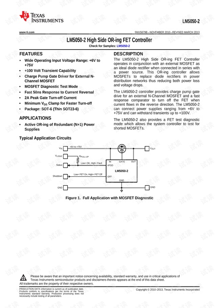

V
IN
V
OUT
GND
OFF
OUT
IN
GATE
LM5050-2
Shutdown
GND
GND
nFGD
Low= FET On, High= FET Off
+6V to +75V
Status
V
LOGIC
Low= OK, High= Fault
R
PULL-UP
LM5050-2
www.ti.com
SNVS679B –NOVEMBER 2010–REVISED MARCH 2013
LM5050-2 High Side OR-ing FET Controller
Check for Samples: LM5050-2
1
FEATURES
DESCRIPTION
The LM5050-2 High Side OR-ing FET Controller
2
• Wide Operating Input Voltage Range: +6V to
operates in conjunction with an external MOSFET as
+75V
an ideal diode rectifier when connected in series with
• +100 Volt Transient Capability
a power source. This OR-ing controller allows
• Charge Pump Gate Driver for External N-
MOSFETs to replace diode rectifiers in power
distribution networks thus reducing both power loss
Channel MOSFET
and voltage drops.
• MOSFET Diagnostic Test Mode
The LM5050-2 controller provides charge pump gate
• Fast 50ns Response to Current Reversal
drive for an external N-Channel MOSFET and a fast
• 2A Peak Gate Turn-off Current
response comparator to turn off the FET when
• Minimum V
DS
Clamp for Faster Turn-off
current flows in the reverse direction. The LM5050-2
can connect power supplies ranging from +6V to
• Package: SOT-6 (Thin SOT23-6)
+75V and can withstand transients up to +100V.
APPLICATIONS
The LM5050-2 also provides a FET test diagnostic
mode which allows the system controller to test for
• Active OR-ing of Redundant (N+1) Power
shorted MOSFETs.
Supplies
Typical Application Circuits
Figure 1. Full Application with MOSFET Diagnostic
1
Please be aware that an important notice concerning availability, standard warranty, and use in critical applications of
Texas Instruments semiconductor products and disclaimers thereto appears at the end of this data sheet.
2All trademarks are the property of their respective owners.
PRODUCTION DATA information is current as of publication date.
Copyright © 2010–2013, Texas Instruments Incorporated
Products conform to specifications per the terms of the Texas
Instruments standard warranty. Production processing does not
necessarily include testing of all parameters.


剩余23页未读,继续阅读
资源评论


