没有合适的资源?快使用搜索试试~ 我知道了~
资源详情
资源评论
资源推荐
© Semiconductor Components Industries, LLC, 2015
May, 2015 − Rev. 9
1 Publication Order Number:
NCV7420/D
NCV7420
LIN Transceiver with 3.3V
or 5 V Voltage Regulator
General Description
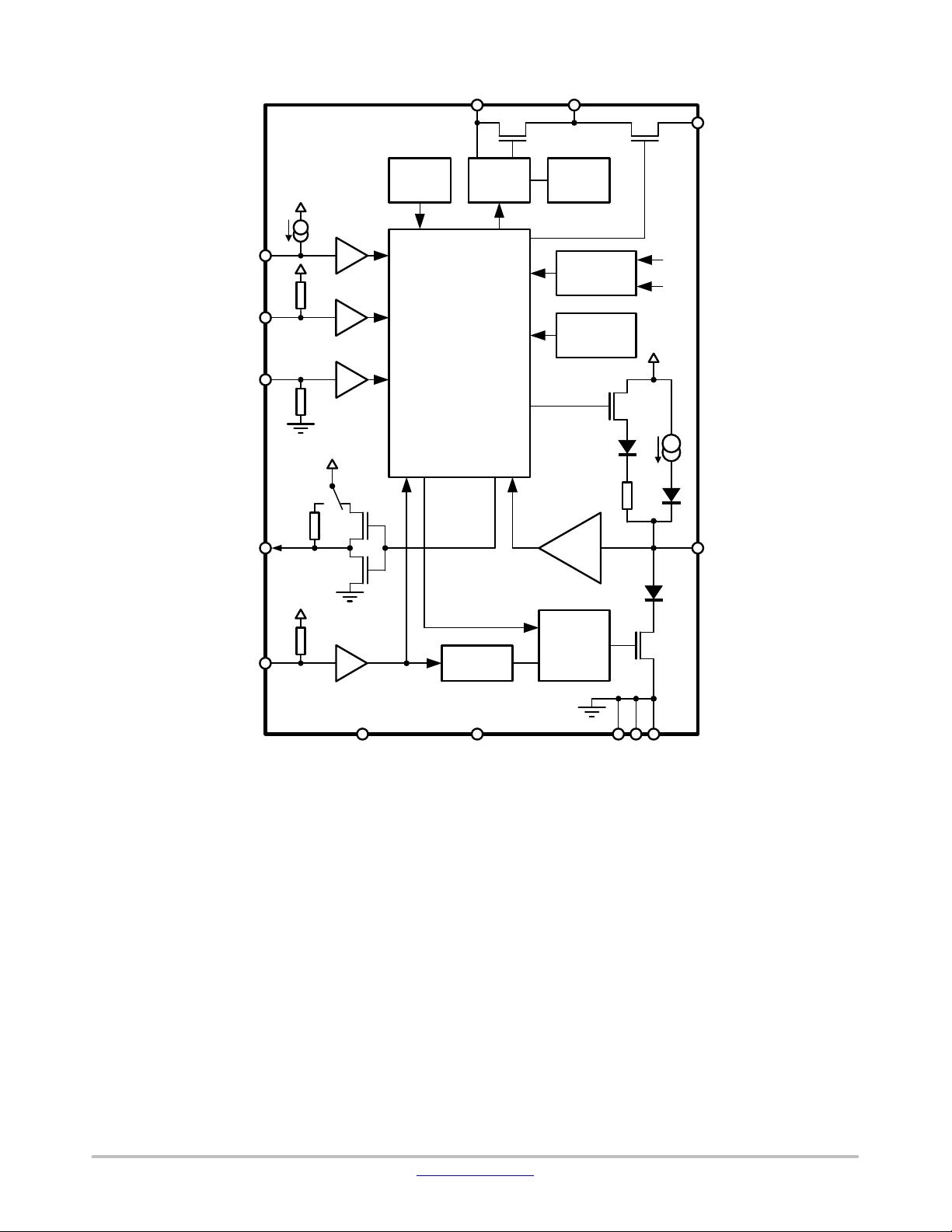
The NCV7420 is a fully featured local interconnect network (LIN)
transceiver designed to interface between a LIN protocol controller
and the physical bus. The transceiver is implemented in I3T
technology enabling both high−voltage analog circuitry and digital
functionality to co−exist on the same chip.
The NCV7420 LIN device is a member of the in−vehicle
networking (IVN) transceiver family of ON Semiconductor that
integrates a LIN v2.0/2.1 physical transceiver and either a 3.3 V or a
5 V voltage regulator.
The LIN bus is designed to communicate low rate data from control
devices such as door locks, mirrors, car seats, and sunroofs at the
lowest possible cost. The bus is designed to eliminate as much wiring
as possible and is implemented using a single wire in each node. Each
node has a slave MCU−state machine that recognizes and translates
the instructions specific to that function. The main attraction of the
LIN bus is that all the functions are not time critical and usually relate
to passenger comfort.
KEY FEATURES
LIN−Bus Transceiver
• LIN compliant to specification revision 2.0 and 2.1
(backward compatible to version 1.3) and J2602
• I3T high voltage technology
• Bus voltage ±45 V
• Transmission rate up to 20 kBaud
Protection
• Thermal shutdown
• Indefinite short−circuit protection on pins LIN and
WAKE towards supply and ground
• Load dump protection (45 V)
• Bus pins protected against transients in an automotive
environment
• System ESD protection level for LIN, WAKE and V
BB
up to ±12 kV
Voltage Regulator
• Output voltage 5 V / ~50 mA or 3.3 V / ~50 mA
• Wake−up input
• Enable inputs for standby and sleep mode
• INH output for auxiliary purposes (switching of an
external pull−up or resistive divider towards battery,
control of an external voltage regulator etc.)
EMI Compatibility
• Integrated slope control
• Meets most demanding EMS/EME requirements
Modes
• Normal mode: LIN communication in either low (up to
10 kBaud) or normal slope
• Sleep mode: V
CC
is switched “off” and no
communication on LIN bus
• Standby mode: V
CC
is switched “on” but there is no
communication on LIN bus
• Wake−up bringing the component from sleep mode into
standby mode is possible either by LIN command or
digital input signal on WAKE pin. Wake−up from LIN
bus can also be detected and flagged when the chip is
already in standby mode.
Quality
• NCV Prefix for Automotive and Other Applications
Requiring Unique Site and Control Change Require−
ments; AEC−Q100 Qualified and PPAP Capable
• These Devices are Pb−Free, Halogen Free/BFR Free
and are RoHS Compliant
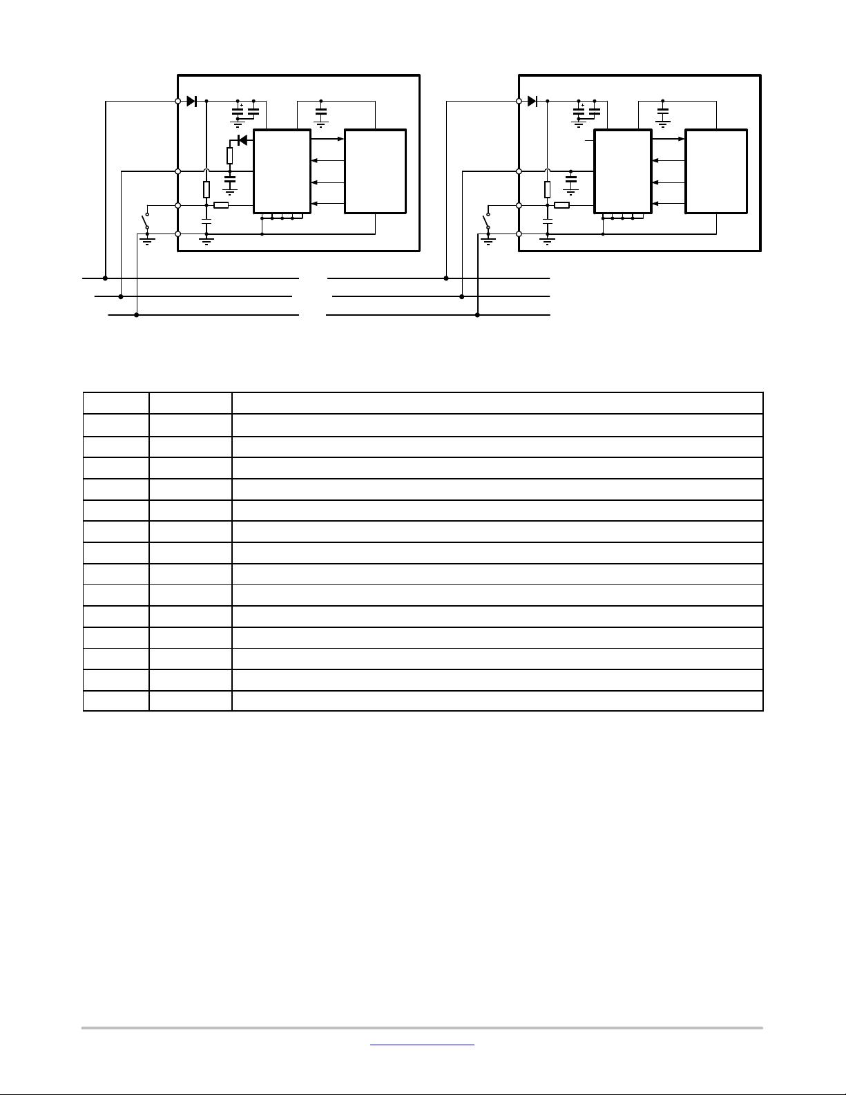
www.onsemi.com
See detailed ordering and shipping information in the package
dimensions section on page 19 of this data sheet.
ORDERING INFORMATION
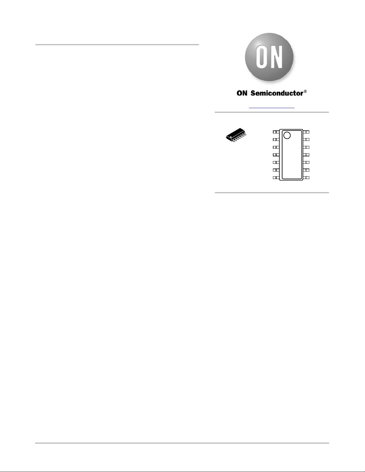
1
14
SOIC−14
D SUFFIX
CASE 751AP
PIN CONFIGURATION
1
2
3
4
14
13
12
11
GND GND
TxD
RxD
GND
LIN
NCV7420
5
6
7
10
9
8
WAKE
OTP_ZAP
INH
TEST
EN
STB
V
CC
V
BB
NCV7420
www.onsemi.com
2
MARKING DIAGRAM
NCV7420−x
AWLYWWG
1
14
NCV7420 = Specific Device Code
−x = −3 = NCV7420D23G
= −4 = NCV7420D24G
= −5 = NCV7420D25G
= −6 = NCV7420D26G
A = Assembly Location
WL = Wafer Lot
Y = Year
WW = Work Week
G = Pb−Free Package
Table 1. KEY TECHNICAL CHARACTERISTICS − 3.3 V version
Symbol Parameter Min Typ Max Unit
V
BB
Nominal battery operating voltage (Note 1) 5 12 26
V
Load dump protection (Note 2) 45
I
BB_SLP
Supply current in sleep mode 20
mA
V
CC_OUT
(Note 4)
Regulated V
CC
output, V
CC
load 1 mA−30 mA 3.23 3.30 3.37
V
Regulated V
CC
output, V
CC
load 0 mA−50 mA 3.19 3.30 3.41
I
OUT_MAX
Maximum V
CC
output current (Note 3) 50 mA
V
WAKE
Operating DC voltage on WAKE pin 0 V
BB
V
Maximum rating voltage on WAKE pin −45 45
T
JSD
Junction thermal shutdown temperature 165 195 °C
T
J
Operating junction temperature −40 +150 °C
Table 2. KEY TECHNICAL CHARACTERISTICS − 5 V version
Symbol Parameter Min Typ Max Unit
V
BB
Nominal battery operating voltage (Note 1) 6 12 26
V
Load dump protection 45
I
BB_SLP
Supply current in sleep mode 20
mA
V
CC_OUT
(Note 4)
Regulated V
CC
output, V
CC
load 1 mA−30 mA 4.9 5.0 5.1
V
Regulated V
CC
output, V
CC
load 0 mA−50 mA 4.83 5.0 5.17
I
OUT_MAX
Maximum V
CC
output current (Note 3) 50 mA
V
WAKE
Operating DC voltage on WAKE pin 0 V
BB
V
Maximum rating voltage on WAKE pin −45 45
T
JSD
Junction thermal shutdown temperature 165 195 °C
T
J
Operating junction temperature −40 +150 °C
1. Below 5 V on V
BB
in normal mode, the bus will either stay recessive or comply with the voltage level specifications and transition time
specifications as required by SAE J2602. It is ensured by the battery monitoring circuit.
2. The applied transients shall be in accordance with ISO 7637 part 1, test pulse 5. The device complies with functional class C; class A can
be reached depending on the application and external conditions.
3. Thermal aspects of the entire end−application have to be taken into account in order to avoid thermal shutdown of NCV7420.
4. V
CC
voltage regulator output must be properly decoupled by external capacitor of min. 8 mF with ESR < 1 W to ensure stability.
Table 3. THERMAL CHARACTERISTICS
Symbol Parameter Conditions Value Unit
R
q
JA1
Thermal resistance junction−to−ambient, 1S0P PCB (Note 5) free air 140 K/W
R
q
JA
2
Thermal resistance junction−to−ambient, 2S2P PCB (Note 6) free air 80 K/W
5. Test board according to EIA/JEDEC Standard JESD51−3, signal layer with 20% trace coverage
6. Test board according to EIA/JEDEC Standard JESD51−7, signal layers with 20% trace coverage
NCV7420
www.onsemi.com
3
Figure 1. Block Diagram
STB
TxD
EN
RxD
WAKE
Control Logic
NCV7420
LIN
Timeout
Driver &
Slope
Control
Thermal
shutdown
Osc
INH
TEST
OTP_ZAP
POR
V−reg
Band−
gap
Receiver
GND
Normal
mode
Standby
Sleep
V
BB
V
CC
V
BB
V
BB
V
CC
V
BB
V
CC
V
CC
V
CC
Typical Application
Application Schematic
The EMC immunity of the Master−mode device can be
further enhanced by adding a capacitor between the LIN
output and ground. The optimum value of this capacitor is
determined by the length and capacitance of the LIN bus, the
number and capacitance of Slave devices, the pull−up
resistance of all devices (Master & Slave), and the required
time constant of the system, respectively.
V
CC
voltage must be properly stabilized by external
capacitor: capacitor of min. 8 mF (ESR < 1 W).
NCV7420
www.onsemi.com
4
Figure 2. Typical Application Diagram
KL30
LIN−BUS
KL31
LIN
Master Node
1 nF
1kW
GND
NCV7420
Micro
controller
GND
INH
V
BB
VBAT
GND
10nF
WAKE
LIN
Slave Node
220pF
GND
Micro
controller
VBAT
GND
WAKE
10uF
V
CC V
CC
10uF
100nF
TESTOTP_ZAP
10nF
GND
INH
V
BB V
CC
TEST
OTP_ZAP
LIN
WAKE
10uF 100nF
V
CC
LIN
WAKE
EN
STB
TxD
RxD
NCV7420
EN
STB
TxD
RxD
10uF
Table 4. PIN DESCRIPTION
Pin Name Description
1 V
BB
Battery supply input
2 LIN LIN bus output/input
3 GND Ground
4 GND Ground
5 WAKE High voltage digital input pin to switch the part from sleep− to standby mode
6 INH Inhibit output
7 OTP_ZAP Supply for programming of trimming bits at factory testing, should be grounded in the application
8 TEST Digital input for factory testing, should be grounded in the application
9 EN Enable input, transceiver in normal operation mode when high
10 STB Standby mode control input
11 GND Ground
12 TxD Transmit data input, low in dominant state
13 RxD Receive data output; low in dominant state; push−pull output
14 V
CC
Supply voltage (output)
Overall Functional Description
LIN is a serial communication protocol that efficiently
supports the control of mechatronic nodes in distributed
automotive applications. The domain is class−A multiplex
buses with a single master node and a set of slave nodes.
NCV7420 is designed as a master or slave node for the
LIN communication interface with an integrated 3.3 V or
5 V voltage regulator having a current capability up to
50 mA for supplying any external components
(microcontroller).
NCV7420 contains the LIN transmitter, LIN receiver,
voltage regulator, power−on−reset (POR) circuits and
thermal shutdown (TSD). The LIN transmitter is optimized
for the maximum specified transmission speed of 20 kBaud
with EMC performance due to reduced slew rate of the LIN
output.
The junction temperature is monitored via a thermal
shutdown circuit that switches the LIN transmitter and
voltage regulator off when temperature exceeds the TSD
trigger level.
NCV7420 has four operating states (normal mode, low
slope mode, standby mode, and sleep mode) that are
determined by the input signals EN, WAKE, STB, and TxD.
Operating States
NCV7420 provides four operating states, two modes for
normal operation with communication, one standby without
communication and one low power mode with very low
current consumption. See Figure 3.
剩余19页未读,继续阅读
weixin_38594687
- 粉丝: 2
- 资源: 967
上传资源 快速赚钱
- 我的内容管理 展开
- 我的资源 快来上传第一个资源
- 我的收益 登录查看自己的收益
- 我的积分 登录查看自己的积分
- 我的C币 登录后查看C币余额
- 我的收藏
- 我的下载
- 下载帮助
安全验证
文档复制为VIP权益,开通VIP直接复制
信息提交成功
评论0