TI方案-信号输入ADC处理-单端信号转差分后到ADC更合理
需积分: 1 37 浏览量
2024-04-01
10:00:47
上传
评论
收藏 136KB PDF 举报

ADC
+IN
–IN
6
U2
4
7
3
2
V
IN
R
1
C
1
0.1 Fμ
C
2
0.1 Fμ
R
2
R
5
R
6
R
3
R
4
–V
S
–V
S
V
OUT
V
OUT
V
REF
+V
S
+V
S
6
U1
4
7
3
2
Application Report
SBAA069B–March 2001–Revised May 2015
Getting the Full Potential from Your ADC
JohnAustin
ABSTRACT
Many of today’s high-resolution ADCs (Analog-to-Digital Converters) are operating from a single supply
and utilize fully differential inputs. This can be a problem for single ended signals that are bipolar relative
to common. This article will illustrate circuit configurations that will preserve the full-scale input range by
utilizing modern features, such as Programmable Gain Amplifiers (PGAs) and internal voltage reference. It
will also discuss issues that the designer must consider when selecting components utilizing these signal-
conditioning circuits.
The differential inputs provide common-mode rejection eliminating much of the system noise imposed on
the input signal. In most converters, the reference inputs determine the full-scale analog input range as
well as the position of bipolar zero of the analog input signal.
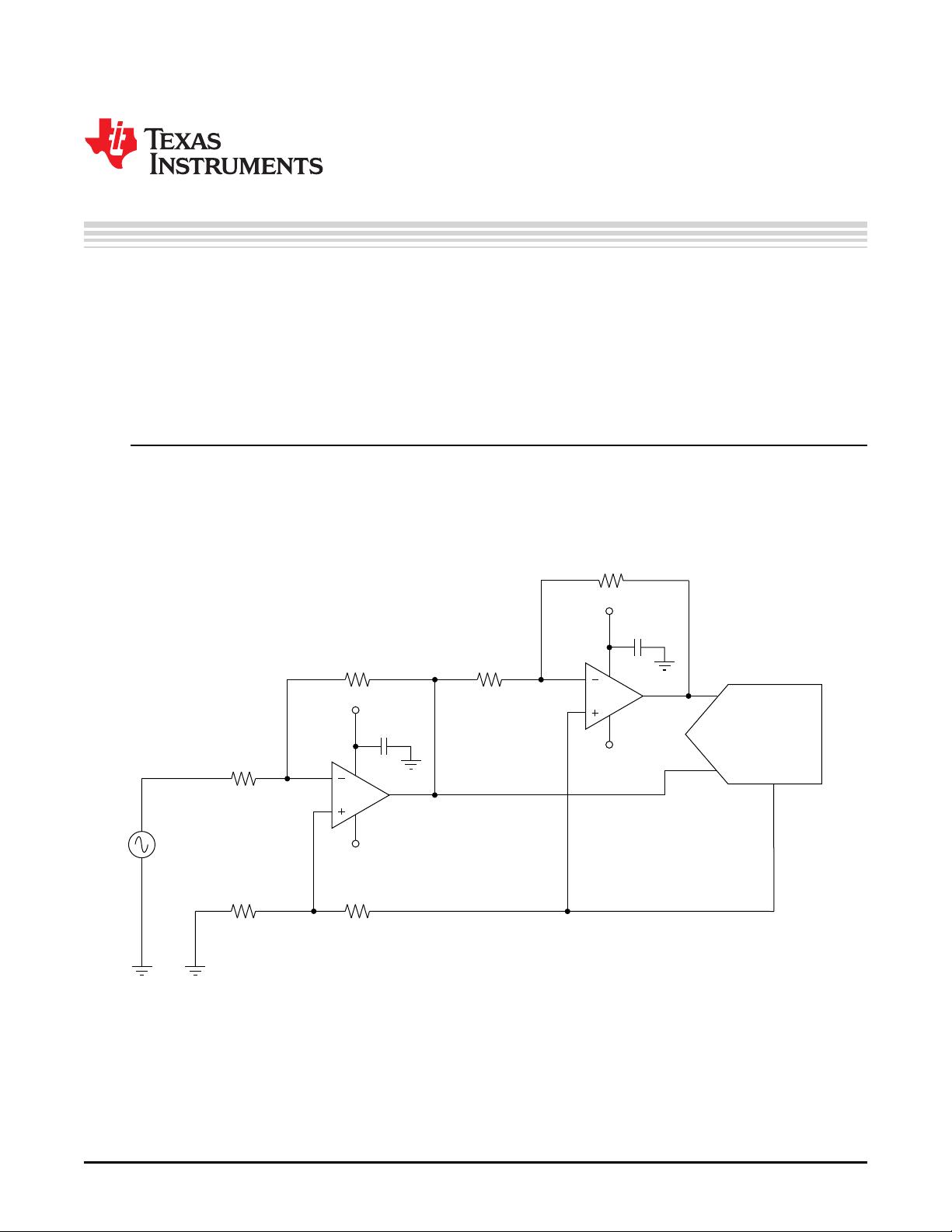
For truly differential input ADCs without a built-in PGA, Figure 1 is a proposed solution.
Figure 1. Circuit Schematic to Convert a Single-Ended Bipolar Input to a Unipolar Differential Output.
All trademarks are the property of their respective owners.
1
SBAA069B–March 2001–Revised May 2015 Getting the Full Potential from Your ADC
Submit Documentation Feedback
Copyright © 2001–2015, Texas Instruments Incorporated
资源评论


