没有合适的资源?快使用搜索试试~ 我知道了~
Hynix -HY62U8100B.pdf
需积分: 9 0 下载量 91 浏览量
2021-04-29
16:30:33
上传
评论
收藏 205KB PDF 举报
温馨提示
试读
13页
Hynix -HY62U8100B.pdf
资源推荐
资源详情
资源评论
This document is a general product description and is subject to change without notice. Hynix Electronics does not assume any
responsibility for use of circuits described. No patent licenses are implied.
Rev 13 / Apr. 2001 Hynix Semiconductor
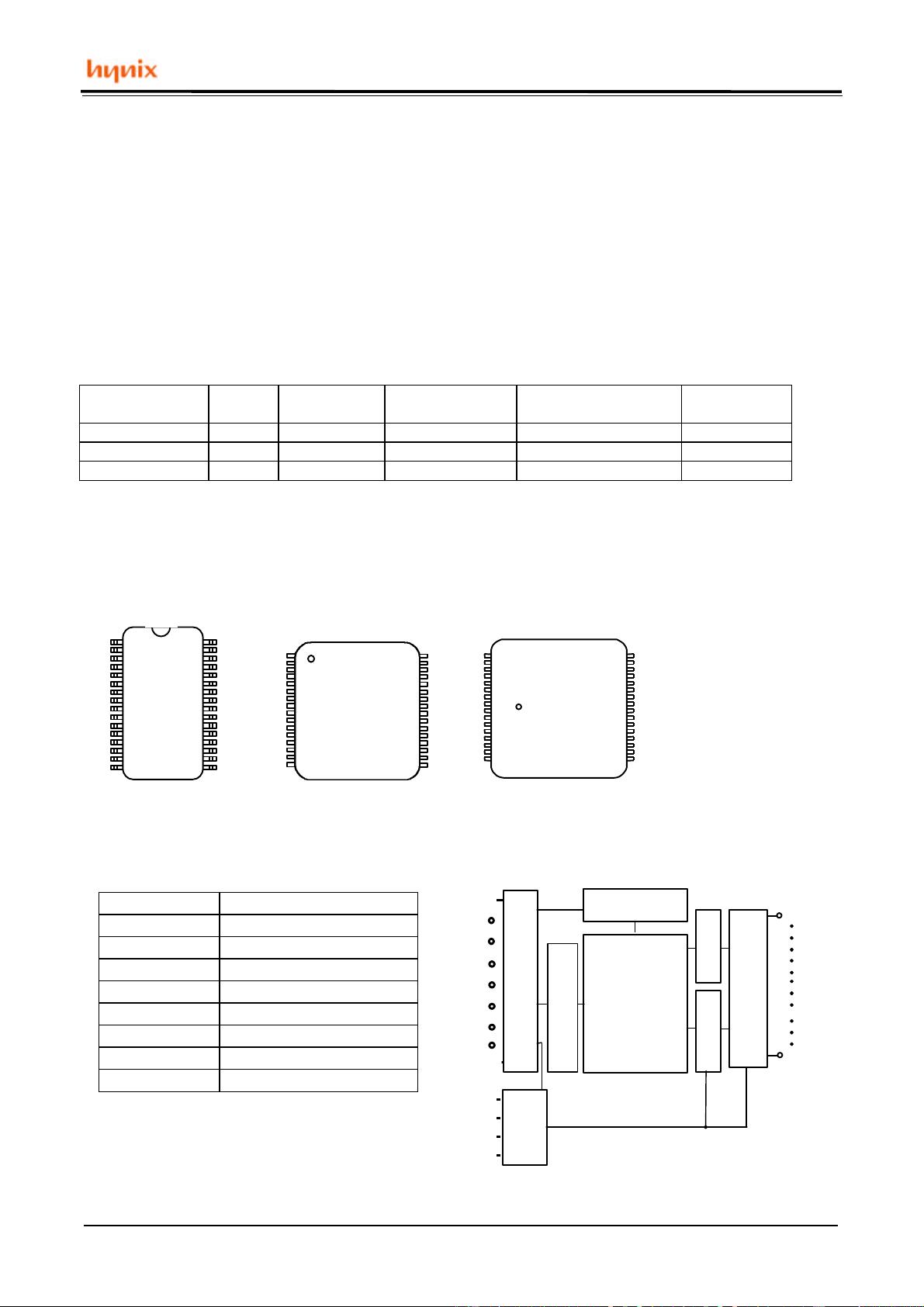
HY62U8100B Series
128Kx8bit CMOS SRAM
Document Title
128K x8 bit 3.0V Low Power CMOS slow SRAM
Revision History
Revision No History Draft Date Remark
10 Initial Revision History Insert Jul.25.2000 Final
Revised
- Insert 70ns Part
11 Change the Notch Location of sTSOP Sep.04.2000 Final
- Left-Top => Left-Center
12 Marking Information Add Dec.04.2000 Final
Revised
- AC Test Condition Add : 5pF Test Load
13 Changed Logo Apr.30.2001 Final
- HYUNDAI -> hynix
- Marking Information Change
HY62U8100B Series
Rev 13 / Apr. 2001
2
DESCRIPTION
The HY62U8100B is a high speed, low power and
1M bit CMOS SRAM organized as 131,072 words
by 8bit. The HY62U8100B uses high performance
CMOS process technology and designed for high
speed low power circuit technology. It is
particulary well suited for used in high density low
power system application. This device has a data
retention mode that guarantees data to remain
valid at a minimum power supply voltage of 2.0V.
FEATURES
• Fully static operation and Tri-state output
• TTL compatible inputs and outputs
• Battery backup(LL-part)
-. 2.0V(min) data retention
• Standard pin configuration
-. 32 - SOP - 525mil
-. 32 - TSOP-I - 8X20(Standard and Reversed)
-. 32 - sTSOP-I - 8X13.4
(Standard and Reversed)
Product Voltage
Speed Operation Standby Current(uA)
Temperature
No. (V) (ns) Current/Icc(mA)
LL
(°C)
HY62U8100B 2.7~3.3
70*/85/100 5 10 0~70
HY62U8100B-E
2.7~3.3
70*/85/100 5 15 -25~85(E)
HY62U8100B-I 2.7~3.3
70*/85/100 5 15 -40~85(I)
Note 1. Blank : Commercial, E : Extended, I : Industrial
2. Current value is max.
* 70ns is available with 30pF test load
PIN CONNECTION
1
2
3
4
5
6
7
8
9
10
11
12
13
14
15
16
32
31
30
29
28
27
26
25
24
23
22
21
20
19
18
17
Vcc
A15
/WE
A13
A8
A9
A11
/OE
A10
/CS1
I/O8
I/O7
I/O6
I/O5
I/O4
NC
A16
A14
A12
A7
A6
A5
A4
A3
A2
A1
A0
I/O1
I/O2
I/O3
Vss
CS2
SOP TSOP-I sTSOP-I
( Standard ) (Standard)
PIN DESCRIPTION BLOCK DIAGRAM
Pin Name Pin Function
/CS1 Chip Select 1
CS2 Chip Select 2
/WE Write Enable
/OE Output Enable
A0 ~ A16 Address Inputs
I/O1 ~ I/O8 Data Inputs / Outputs
Vcc Power(2.7V~3.3V)
Vss Ground
MEMORY ARRAY
128K x 8
ROW
DECODER
SENSE AMP
WRITE DRIVER
DATA I/O
BUFFER
I/O1
I/O8
COLUMN
DECODER
ADD INPUT
BUFFER
A0
A16
COLUMN
DECODER
/CS1
CS2
/OE
/WE
1
2
3
4
5
6
7
8
9
10
11
12
13
14
15
16
32
31
30
29
28
27
26
25
24
23
22
21
20
19
18
17
/OE
A10
DQ8
DQ7
DQ6
DQ5
DQ4
Vss
DQ3
DQ2
DQ1
A0
A1
A2
A3
A11
A9
A8
A13
/WE
CS2
A15
Vcc
NC
A16
A14
A12
A7
A6
A5
A4
/CS1
A11
A9
A8
A13
/WE
CS2
A15
Vcc
NC
A16
A14
A12
A7
A6
A5
A4
/
OE
A10
/CS1
DQ8
DQ7
DQ6
DQ5
DQ4
Vss
DQ3
DQ2
DQ1
A0
A1
A2
A3
1
2
3
4
5
6
7
8
9
10
11
12
13
14
15
16
32
31
30
29
28
27
26
25
24
23
22
21
20
19
18
17
HY62U8100B Series
Rev 13 / Apr. 2001
2
ORDERING INFORMATION
Part No. Speed Power
Temp.
Package
HY62U8100BLLG 70*/85/100 LL-part SOP
HY62U8100BLLT1 70*/85/100 LL-part TSOP-I(Standard)
HY62U8100BLLR1 70*/85/100 LL-part TSOP-I(Reversed)
HY62U8100BLLST 70*/85/100 LL-part smaller TSOP-I(Standard)
HY62U8100BLLSR 70*/85/100 LL-part smaller TSOP-I(Reversed)
HY62U8100BLLG-E 70*/85/100 LL-part E SOP
HY62U8100BLLT1-E 70*/85/100 LL-part E TSOP-I(Standard)
HY62U8100BLLR1-E 70*/85/100 LL-part E TSOP-I(Reversed)
HY62U8100BLLST-E 70*/85/100 LL-part E Smaller TSOP-I(Standard)
HY62U8100BLLSR-E 70*/85/100 LL-part E Smaller TSOP-I(Reversed)
HY62U8100BLLG-I 70*/85/100 LL-part I SOP
HY62U8100BLLT1-I 70*/85/100 LL-part I TSOP-I(Standard)
HY62U8100BLLR1-I 70*/85/100 LL-part I TSOP-I(Reversed)
HY62U8100BLLST-I 70*/85/100 LL-part I Smaller TSOP-I(Standard)
HY62U8100BLLSR-I 70*/85/100 LL-part I Smaller TSOP-I(Reversed)
Note 1. Blank : Commercial, E : Extended, I : Industrial
* 70ns is available with 30pF test load
ABSOLUTE MAXIMUM RATING (1)
Symbol Parameter Rating Unit Remark
Vcc, VIN, VOUT
Power Supply, Input/Output Voltage -0.3 to 4.6 V
TA Operating Temperature 0 to 70
°C
HY62U8100B
-25 to 85
°C
HY62U8100B-E
-40 to 85
°C
HY62U8100B-I
TSTG Storage Temperature -65 to 125
°C
PD Power Dissipation 10 W
IOUT Data Output Current 50 mA
TSOLDER Lead Soldering Temperature & Time
260 • 10 °C•sec
Note
1. Stresses greater than those listed under ABSOLUTE MAXIMUM RATINGS may cause permanent
damage to the device. This is stress rating only and the functional operation of the device under these or
any other conditions above those indicated in the operation of this specification is not implied.
Exposure to the absolute maximum rating conditions for extended period may affect reliability.
TRUTH TABLE
/CS1
CS2
/WE
/OE
Mode I/O Power
H X X X Deselected High-Z Standby
X L X X Deselected High-Z Standby
L H H H Output Disabled High-Z Active
L H H L Read Data Out Active
L H L X Write Data In Active
Note :
1. H=VIH, L=VIL, X=don't care( VIH or VIL )
剩余12页未读,继续阅读
资源评论
LC灵灵
- 粉丝: 1
- 资源: 261
上传资源 快速赚钱
- 我的内容管理 展开
- 我的资源 快来上传第一个资源
- 我的收益 登录查看自己的收益
- 我的积分 登录查看自己的积分
- 我的C币 登录后查看C币余额
- 我的收藏
- 我的下载
- 下载帮助
安全验证
文档复制为VIP权益,开通VIP直接复制
信息提交成功