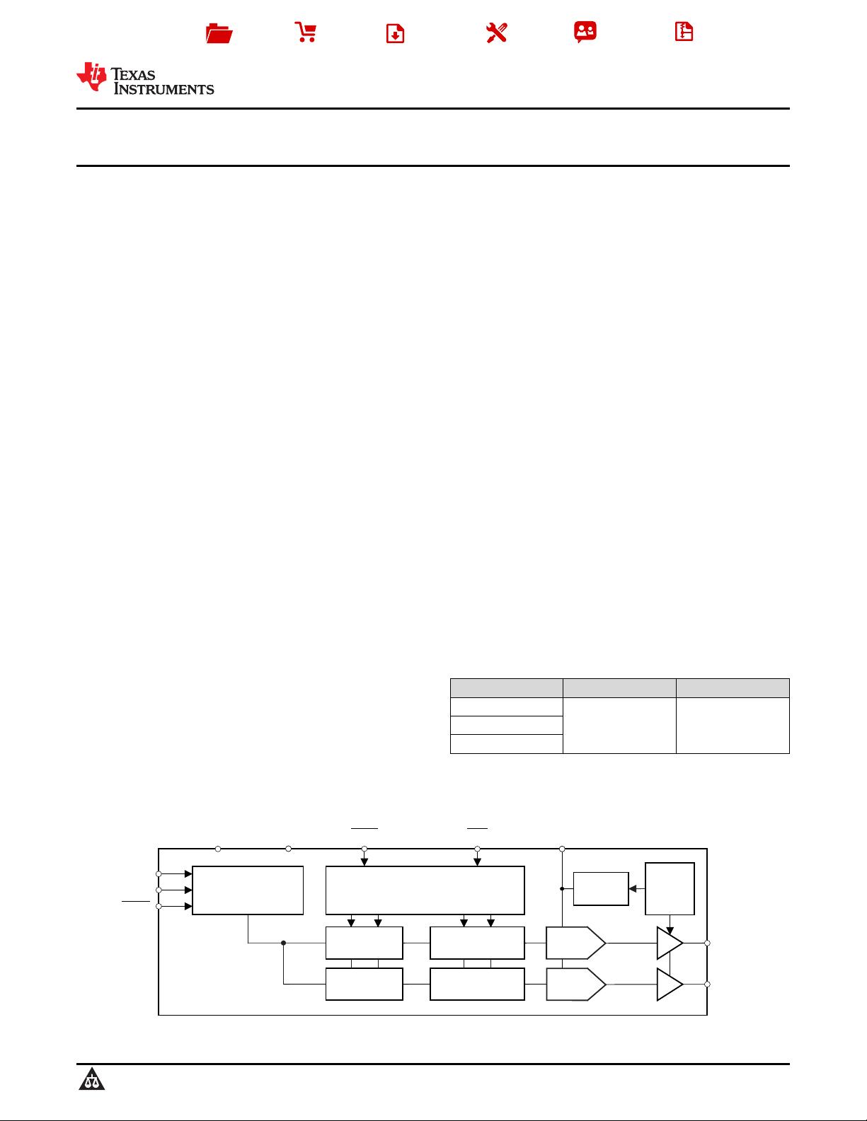
DAC756x (12-Bit)
DAC816x (14-Bit)
DAC856x (16-Bit)
Buffer Control Register Control
Control Logic
Power-
Down
Control
Logic
AV
DD
V
REFIN REFOUT
/V
CLRLDAC
2.5-V
Reference
V B
OUT
V A
OUT
GND
DAC
DAC
Input Control Logic
SYNC
SCLK
D
IN
Data Buffer A
Data Buffer B
DAC Register A
DAC Register B
Product
Folder
Sample &
Buy
Technical
Documents
Tools &
Software
Support &
Community
Reference
Design
DAC7562
,
DAC7563
,
DAC8162
DAC8163
,
DAC8562
,
DAC8563
SLAS719E –AUGUST 2010–REVISED JUNE 2015
DACxx6x Dual 16-, 14-, 12-Bit, Low-Power, Buffered, Voltage-Output
DACs With 2.5-V, 4-PPM/°C Internal Reference
1 Features 3 Description
The DAC756x, DAC816x, and DAC856x devices are
1
• Relative Accuracy:
low-power, voltage-output, dual-channel, 16-, 14-,
– DAC756x (12-Bit): 0.3 LSB INL
and 12-bit digital-to-analog converters (DACs),
– DAC816x (14-Bit): 1 LSB INL
respectively. These devices include a 2.5-V,
4-ppm/°C internal reference, giving a full-scale output
– DAC856x (16-Bit): 4 LSB INL
voltage range of 2.5 V or 5 V. The internal reference
• Glitch Impulse: 0.1 nV-s
has an initial accuracy of ±5 mV and can source or
• Bidirectional Reference: Input or 2.5-V Output
sink up to 20 mA at the V
REFIN
/V
REFOUT
pin.
– Output Disabled by Default
These devices are monotonic, providing excellent
– ±5-mV Initial Accuracy (Max)
linearity and minimizing undesired code-to-code
transient voltages (glitch). They use a versatile three-
– 4-ppm°C Temperature Drift (Typ)
wire serial interface that operates at clock rates up to
– 10-ppm/°C Temperature Drift (Max)
50 MHz. The interface is compatible with standard
– 20-mA Sink and Source Capability
SPI™, QSPI™, Microwire, and digital signal
processor (DSP) interfaces. The DACxx62 devices
• Power-On Reset to Zero Scale or Mid-Scale
incorporate a power-on-reset circuit that ensures the
• Low-Power: 4 mW (Typ, 5-V AV
DD
, Including
DAC output powers up and remains at zero scale
Internal Reference Current)
until a valid code is written to the device, whereas the
• Wide Power-Supply Range: 2.7 V to 5.5 V
DACxx63 devices similarly power up at mid-scale.
These devices contain a power-down feature that
• 50-MHz SPI With Schmitt-Triggered Inputs
reduces current consumption to typically 550 nA at
• LDAC and CLR Functions
5 V. The low power consumption, internal reference,
• Output Buffer With Rail-to-Rail Operation
and small footprint make these devices ideal for
• Packages: WSON-10 (3 mm × 3 mm), VSSOP-10
portable, battery-operated equipment.
• Temperature Range: –40°C to 125°C
The DACxx62 devices are drop-in and function-
compatible with each other, as are the DACxx63
2 Applications
devices. The entire family is available in MSOP-10
and SON-10 packages.
• Portable Instrumentation
• PLC Analog Output Module
Device Information
(1)
• Closed-Loop Servo Control
PART NUMBER PACKAGE BODY SIZE (NOM)
• Voltage Controlled Oscillator Tuning
DAC8562
VSSOP (10),
• Data Acquisition Systems
DAC8162 3.00 mm × 3.00 mm
WSON (10)
• Programmable Gain and Offset Adjustment
DAC7562
(1) For all available packages, see the orderable addendum at
the end of the data sheet.
Simplified Block Diagram
1
An IMPORTANT NOTICE at the end of this data sheet addresses availability, warranty, changes, use in safety-critical applications,
intellectual property matters and other important disclaimers. PRODUCTION DATA.


