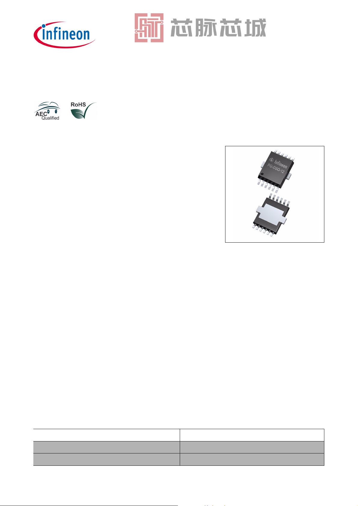
没有合适的资源?快使用搜索试试~ 我知道了~
TLE4473G V53 英飞凌芯片 INFINEON 中文版规格书手册.pdf
需积分: 5 1 下载量 69 浏览量
2023-07-06
10:19:37
上传
评论
收藏 296KB PDF 举报
温馨提示
试读
16页
TLE4473G V53 英飞凌芯片 INFINEON 中文版规格书手册
资源推荐
资源详情
资源评论
Type Package
TLE 4473 GV53 PG-DSO-12
TLE 4473 GV52 PG-DSO-12
Dual Low Drop Voltage Regulator TLE 4473 GV53
TLE 4473 GV52
Data Sheet 1 Rev. 1.1, 2008-09-19
Features
• Output 1: 300 mA, 3.3 V (±3%) or 2.6 V (±3%)
• Output 2: 180 mA, 5 V (±2%)
• Low quiescent current consumption
• Disable function separately for both outputs
• Wide operation range: up to 42 V
• Very low dropout voltage
• 2 independent reset circuits
• Watchdog
• Output protected against short circuit
• Wide temperature range: -40 °C to 150 °C
• Overtemperature protection
• Overload protection
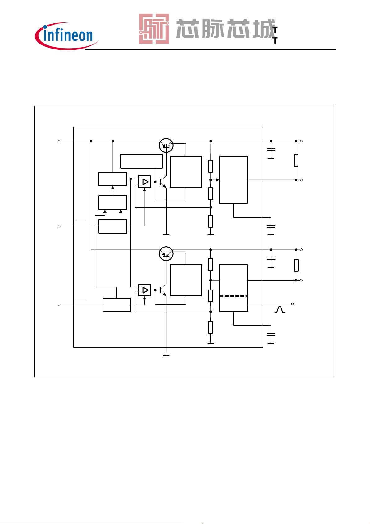
Functional Description
The TLE 4473 is a monolithic integrated voltage regulator with two very low-drop
outputs, Q1 for loads up to 300 mA and Q2 providing a maximum of 180 mA. An input
voltage in the range of 5.6 V ≤
V
I
≤ 45 V is transformed to V
Q2
= 5.0 V (±2%) and
V
Q1
=3.3V ±3% (TLE 4473 GV53) or V
Q1
= 2.6 V ±3% (TLE 4473 GV52). The device is
also available with dual 5 V output voltage, please refer to the TLE 4473 GV55 data
sheet. Two inhibit pins allow a flexible power management. Both outputs can
independently be enabled or disabled. Thus the current consumption of the application
can be reduced to a minimum. The quiescent current of the TLE 4473 with both outputs
disabled is < 1 µA. The TLE 4473 is designed to supply microprocessor systems and
sensors under the severe conditions of automotive applications and is therefore
equipped with additional protection functions against overload, short circuit and
overtemperature.
The device operates in the wide junction temperature range of -40 °C to 150 °C.
Data Sheet 2 Rev. 1.1, 2008-09-19
TLE 4473 GV53
TLE 4473 GV52
The low drop regulator features a reset with adjustable power on delay for each of the
outputs. In addition the output for the microcontroller supply comes up with a watchdog
in order to supervise a microcontroller.
Figure 1 Block Diagram with Typical External Components
AEB03507.VSD
TLE 4473 GV53 / TLE 4473 GV52
Reset
Generator
Reset
Generator
Watchdog
Current and
Saturation
Control,
Overcurrent
Protection
Overtemperature
Shutdown
Bandgap
Reference
Inhibit
Current and
Saturation
Control,
Overcurrent
Protection
Inhibit
10
µF
4.7 kΩ
4
2
Q2
RO2
e. g. µC I/O
or Sensor
Supply
100 nF
10D2
3RO1
5Q1
22 µF
or
10 µF
µC Core
Supply
µC
Reset
100 nF
11D1
GND
6, 12
4.7 kΩ
Ignition
µC
V
Bat
INH29
I
7
INH18
?1
1WI
Watchdog
(from µC)
TLE 4473 GV53
TLE 4473 GV52
Data Sheet 3 Rev. 1.1, 2008-09-19
Reset and Watchdog Behaviour:
The reset output RO1 is in high-state if the voltage on the delay capacitor
C
D1
is greater
or equal
V
DL1
. The delay capacitor C
D1
is charged with the current I
DC1
for output voltages
greater than the reset threshold
V
RT1
. If the output voltage drops below V
RT1
(“reset
condition”), the delay capacitor
C
D1
will be discharged rapidly. If V
D1
reaches V
DL1
, the
reset output RO1 is set to low.
At power-on, the charging process of
C
D1
starts from 0 V, which leads to the equation
(1)
for the power-on reset delay time.
When the voltage at the delay capacitor has reached
V
DU1
and RO1 was set to high, the
watchdog circuit is enabled and discharges
C
D1
with the constant current I
DD1
.
If there is no rising edge observed at the watchdog input,
C
D1
will be discharged down to
V
DL1
, where the reset output RO1 will be set to low and C
D1
will be charged again with
the current
I
DC1
until V
D1
reaches V
DU1
and reset will be set high again.
If a watchdog pulse (rising edge at watchdog input WI) occurs during the discharge
period,
C
D1
is charged again and the reset output stays high. After V
D1
has reached V
DU1
,
the periodical cycle starts again.
The watchdog timing is shown in Figure 2. The maximum duration between two
watchdog pulses corresponds to the minimum watchdog trigger time T
WI,tr
. Higher
capacitances on pin D1 result in larger watchdog trigger time:
(2)
If the output voltage Q2 decreases below
V
RT2
, the external capacitor C
D2
is discharged.
When the voltage at this capacitor drops below
V
DL2
, a reset signal is generated at pin
11 (RO2), i.e. the reset output is set to low-level. If the output voltage rises above the
reset threshold,
C
D2
will be charged with the constant current I
DC2
. After the power-on-
reset time, the voltage at the capacitor reaches
V
DU2
and the reset output will be set to
high again. The value of the power-on-reset time can be set within a wide range
depending of the capacitance of
C
D2
using Equation (1) analogous for Q2.
t
Don,
C
D1
V
DU1
×
I
DC1
-----------------------------=
T
WI,tr
max
0.42 ms/nF C
D1
×=
Data Sheet 4 Rev. 1.1, 2008-09-19
TLE 4473 GV53
TLE 4473 GV52
Figure 2 Watchdog Timing Schedule
AED03099_4473gv53
W
V
V
V
Q
D1
V
V
WO
V
DU1
-
V
DL1
()
Ι
(
DC1
+
DD1
)
Ι
Ι
DC1
Ι
x
DD1
T
WD, p
=
WD, L
t
WD, p
T
WI, tr
T
WD, L
t
=
V
V
(
DU1
-
DL1
)
Ι
DC1
T
=
V
V
(
DU1
-
DL1
)
Ι
DD1
DU1
V
V
DL1
Ι
Ι
WI, tr
C
D1
;;
D1
C
D1
C
t
t
t
t
t
剩余15页未读,继续阅读
资源评论
芯脉芯城
- 粉丝: 3
- 资源: 4031
上传资源 快速赚钱
- 我的内容管理 展开
- 我的资源 快来上传第一个资源
- 我的收益 登录查看自己的收益
- 我的积分 登录查看自己的积分
- 我的C币 登录后查看C币余额
- 我的收藏
- 我的下载
- 下载帮助
安全验证
文档复制为VIP权益,开通VIP直接复制
信息提交成功