没有合适的资源?快使用搜索试试~ 我知道了~
IMBF170R650M1 INFINEON 英飞凌芯片 中文版规格书手册.pdf
需积分: 5 0 下载量 60 浏览量
2023-06-19
15:58:53
上传
评论
收藏 1.2MB PDF 举报
温馨提示
试读
15页
IMBF170R650M1 INFINEON 英飞凌芯片 中文版规格书手册
资源推荐
资源详情
资源评论
Datasheet Please read the Important Notice and Warnings at the end of this document
www.infineon.com page 1 of 15 2020-04-27
IMBF170R650M1
IMBF170R650M1
CoolSiC™ 1700V SiC Trench MOSFET
Silicon Carbide MOSFET
Features
Revolutionary semiconductor material - Silicon Carbide
Optimized for fly-back topologies
12V/0V gate-source voltage compatible with most fly-back controllers
Very low switching losses
Benchmark gate threshold voltage, V
GS(th)
= 4.5V
Fully controllable dV/dt for EMI optimization
Benefits
Reduction of system complexity
Directly drive from fly-back controller
Efficiency improvement and cooling effort reduction
Enabling higher frequency
Potential applications
Energy generation
o Solar string inverter
o Solar Central inverter
Industrial power supplies
o Industrial UPS
o Industrial SMPS
Infrastructure – Charger
o Charger
Product validation
Qualified for industrial applications according to the relevant tests of JEDEC 47/20/22
Note: the source and sense pins are not exchangeable, their exchange might lead to malfunction
recommended for forward operation mode only
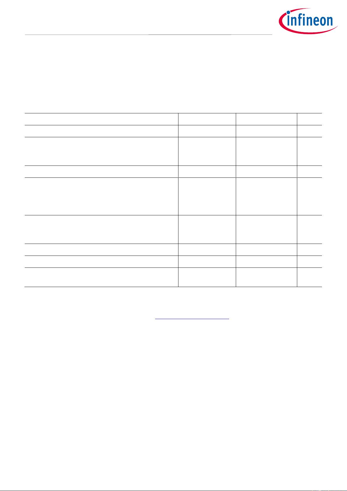
Table 1 Key Performance and Package Parameters
Type
V
DS
I
D
T
C
= 25°C, R
th(j-c,max)
R
DS(on)
T
vj
= 25°C, I
D
= 1.5A, V
GS
= 12V
T
vj,max
Marking
Package
IMBF170R650M1
1700V
7.4A
650mΩ
175°C
170M1650
PG-TO263-7
Drain
Source
pin 3~7
Gate
pin 1
Sense
pin 2
Datasheet 2 of 15 2.1
2020-04-27
IMBF170R650M1
CoolSiC™ 1700V SiC Trench MOSFET
1700V SiC Trench MOSFET
Table of contents
Table of contents
Features ........................................................................................................................................ 1
Benefits ......................................................................................................................................... 1
Potential applications ..................................................................................................................... 1
Product validation .......................................................................................................................... 1
Table of contents ............................................................................................................................ 2
1 Maximum ratings ................................................................................................................... 3
2 Thermal resistances ............................................................................................................... 4
3 Electrical Characteristics ........................................................................................................ 5
3.1 Static characteristics ............................................................................................................................... 5
3.2 Dynamic characteristics .......................................................................................................................... 6
3.3 Switching characteristics ........................................................................................................................ 7
4 Electrical characteristic diagrams ............................................................................................ 8
5 Package drawing ................................................................................................................... 12
6 Test conditions ..................................................................................................................... 13
Revision history............................................................................................................................. 14
Datasheet 3 of 15 2.1
2020-04-27
IMBF170R650M1
CoolSiC™ 1700V SiC Trench MOSFET
Maximum ratings
1 Maximum ratings
For optimum lifetime and reliability, Infineon recommends operating conditions that do not exceed 80% of the
maximum ratings stated in this datasheet.
Table 2 Maximum ratings
Parameter
Symbol
Value
Unit
Drain-source voltage, T
vj
≥ 25°C
V
DSS
1700
V
DC drain current for R
th(j-c,max)
, limited by T
vjmax
, V
GS
= 12V,
T
C
= 25°C
T
C
= 100°C
I
D
7.4
5.2
A
Pulsed drain current, t
p
limited by T
vjmax
, V
GS
= 12V
I
D,pulse
1
18.7
A
Gate-source voltage
2
Max transient voltage, < 1% duty cycle
Recommended turn-on gate voltage
Recommended turn-off gate voltage
V
GS
V
GS,on
V
GS,off
-10… 20
12… 15
0
V
Power dissipation, limited by T
vjmax
T
C
= 25°C
T
C
= 100°C
P
tot
88
44
W
Virtual junction temperature
T
vj
-55… 175
°C
Storage temperature
T
stg
-55… 150
°C
Soldering temperature
Reflow soldering (MSL1 according to JEDEC J-STD-020)
T
sold
260
°C
1
verified by design
2
Important note: The selection of positive and negative gate-source voltages impacts the long-term behavior
of the device. The design guidelines described in Application Note AN2018-09 must be considered to ensure
sound operation of the device over the planned lifetime.
剩余14页未读,继续阅读
资源评论
芯脉芯城
- 粉丝: 3
- 资源: 4031
上传资源 快速赚钱
- 我的内容管理 展开
- 我的资源 快来上传第一个资源
- 我的收益 登录查看自己的收益
- 我的积分 登录查看自己的积分
- 我的C币 登录后查看C币余额
- 我的收藏
- 我的下载
- 下载帮助
安全验证
文档复制为VIP权益,开通VIP直接复制
信息提交成功