IPP60R022S7 INFINEON 英飞凌芯片 中文版规格书手册.pdf
需积分: 5 92 浏览量
2023-06-12
10:15:16
上传
评论
收藏 1.56MB PDF 举报

1
IPP60R022S7
Rev.2.0,2019-05-07Final Data Sheet
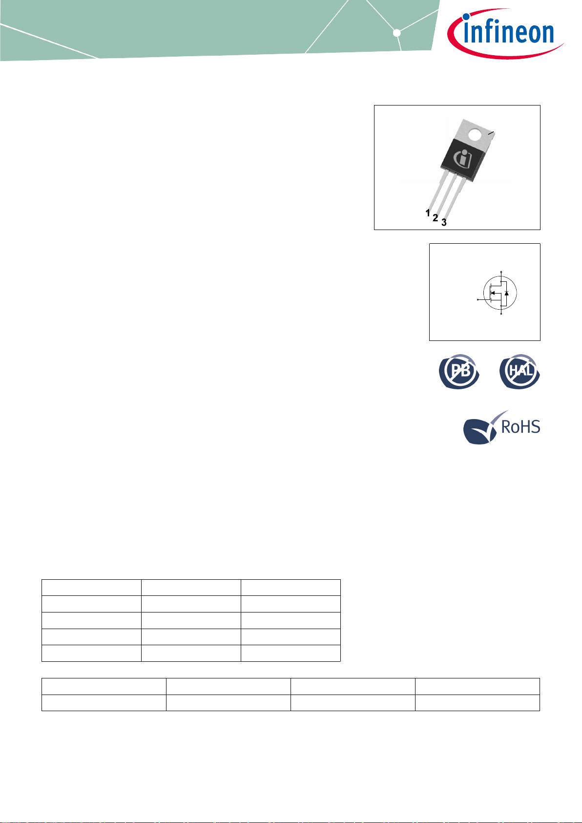
tab
PG-TO220
Drain
Pin 2, Tab
Gate
Pin 1
Source
Pin 3
*1
*1: Internal body diode
MOSFET
600VCoolMOSªSJS7PowerDevice
IPP60R022S7enablesthebestpriceperformanceforlowfrequency
switchingapplications.CoolMOS™S7boaststhelowestRdsonvaluesfor
aHVSJMOSFET,withdistinctiveincreaseofenergyefficiency.
CoolMOS™S7isoptimizedfor“staticswitching”andhighcurrent
applications.Itisanidealfitforsolidstaterelayandcircuitbreakerdesigns
aswellasforlinerectificationinSMPSandinvertertopologies.
Features
•CoolMOS™S7technologyenables22mΩR
DS(on)
inthesmallestfootprint
•Optimizedpriceperformanceinlowfrequencyswitchingapplications
•Highpulsecurrentcapability
•TO220packagewithtotalPb-freedieattach
Benefits
•Minimizedconductionlosses(eliminate/reduceheatsink)
•Increasedsystemperformance
•Morecompactandeasierdesign
•LowerBOMor/andTCOoverprolongedlifetime
Comparedtoelectromechanicaldevices:
•Fasterswitchingtimes
•Morereliabilityandlongersystemlifetime
•Shock&Vibrationresistance
•Nocontactarcing,bouncingordegradationoverlifetime
Potentialapplications
•Solidstaterelaysandcircuitbreakers
•Linerectificationinhighpower/performanceapplicationse.g.Computing,
Telecom,UPSandSolar
Productvalidation
FullyqualifiedaccordingtoJEDECforIndustrialApplications
Pleasenote:ForMOSFETparallelingtheuseofferritebeadsonthegate
orseparatetotempolesisgenerallyrecommended.
Table1KeyPerformanceParameters
Parameter Value Unit
R
DS(on),max
22 mΩ
Q
g,typ
150 nC
V
SD
0.83 V
Pulsed I
SD
, I
DS
375 A
Type/OrderingCode Package Marking RelatedLinks
IPP60R022S7 PG-TO 220-3 60R022S7 see Appendix A

剩余13页未读,继续阅读
资源评论


