IPP60R060P7 INFINEON 英飞凌芯片 中文版规格书手册.pdf
需积分: 5 88 浏览量
2023-06-09
11:07:26
上传
评论
收藏 1.65MB PDF 举报

1
IPP60R060P7
Rev.2.1,2018-05-15Final Data Sheet
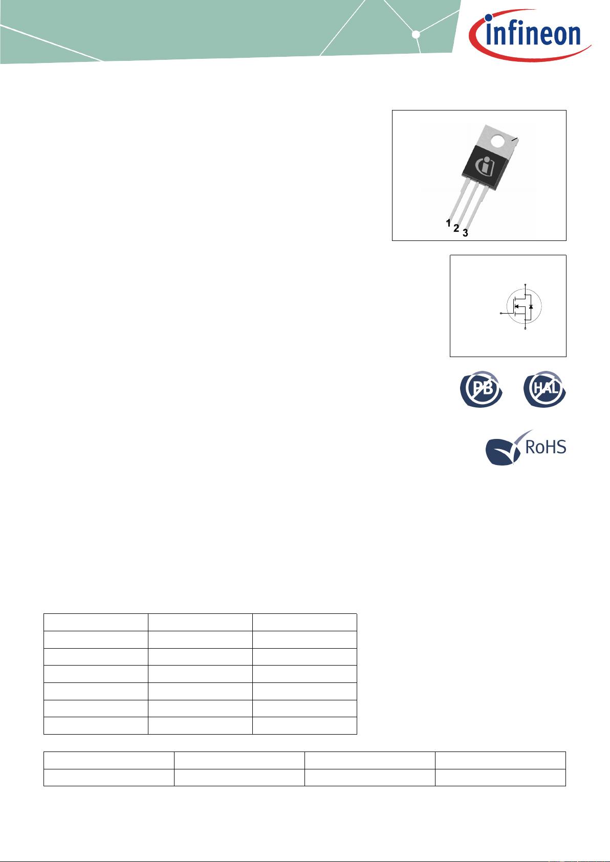
tab
PG-TO220
Drain
Pin 2, Tab
Gate
Pin 1
Source
Pin 3
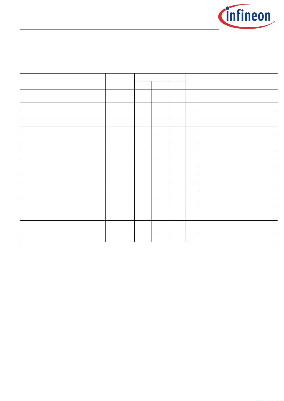
MOSFET
600VCoolMOSªP7PowerTransistor
TheCoolMOS™7thgenerationplatformisarevolutionarytechnologyfor
highvoltagepowerMOSFETs,designedaccordingtothesuperjunction
(SJ)principleandpioneeredbyInfineonTechnologies.The600V
CoolMOS™P7seriesisthesuccessortotheCoolMOS™P6series.It
combinesthebenefitsofafastswitchingSJMOSFETwithexcellentease
ofuse,e.g.verylowringingtendency,outstandingrobustnessofbody
diodeagainsthardcommutationandexcellentESDcapability.
Furthermore,extremelylowswitchingandconductionlossesmake
switchingapplicationsevenmoreefficient,morecompactandmuch
cooler.
Features
•Suitableforhardandsoftswitching(PFCandLLC)duetoanoutstanding
commutationruggedness
•Significantreductionofswitchingandconductionlosses
•ExcellentESDrobustness>2kV(HBM)forallproducts
•BetterR
DS(on)
/packageproductscomparedtocompetitionenabledbya
lowR
DS(on)
*A(below1Ohm*mm²)
•Fullyqualifiedacc.JEDECforIndustrialApplications
Benefits
•Easeofuseandfastdesign-inthroughlowringingtendencyandusage
acrossPFCandPWMstages
•Simplifiedthermalmanagementduetolowswitchingandconduction
losses
•Increasedpowerdensitysolutionsenabledbyusingproductswith
smallerfootprintandhighermanufacturingqualitydueto>2kVESD
protection
•Suitableforawidevarietyofapplicationsandpowerranges
Potentialapplications
PFCstages,hardswitchingPWMstagesandresonantswitchingstages
fore.g.PCSilverbox,Adapter,LCD&PDPTV,Lighting,Server,Telecom
andUPS.
Pleasenote:ForMOSFETparallelingtheuseofferritebeadsonthegate
orseparatetotempolesisgenerallyrecommended.
Table1KeyPerformanceParameters
Parameter Value Unit
V
DS
@ T
j,max
650 V
R
DS(on),max
60 mΩ
Q
g,typ
67 nC
I
D,pulse
151 A
E
oss
@ 400V 7.1 µJ
Body diode di
F
/dt 900 A/µs
Type/OrderingCode Package Marking RelatedLinks
IPP60R060P7 PG-TO 220-3 60R060P7 see Appendix A

剩余13页未读,继续阅读
资源评论


芯脉芯城
- 粉丝: 3
- 资源: 4031


最新资源
- VerilogVHDL\FPGA入门教程FPGA器件边练边学-快速入门Verilogvhdl
- 基于C++的mfc的仿QQ聊天系统(高分课程设计期末大作业)
- 基于Java web的学生管理系统(源码+数据库+报告)高分项目
- 基于Java web的学生管理系统(源码+数据库+报告)期末大作业&课程设计
- FM1702SL芯片13.56MHZ NFC读卡器开发板PROTELPCB图+FM1702SL中文说明书+FM1715编程指南
- 期末大作业交通数据分析与应用期末作业程序源码+实验报告.zip
- 期末大作业基于Java web的图书销售管理系统(源码+数据库)高分项目
- python-leetcode面试题解之第274题H指数.zip
- python-leetcode面试题解之第270题最接近二叉搜索树值.zip
- python-leetcode面试题解之第267题回文排列II.zip
资源上传下载、课程学习等过程中有任何疑问或建议,欢迎提出宝贵意见哦~我们会及时处理!
点击此处反馈


