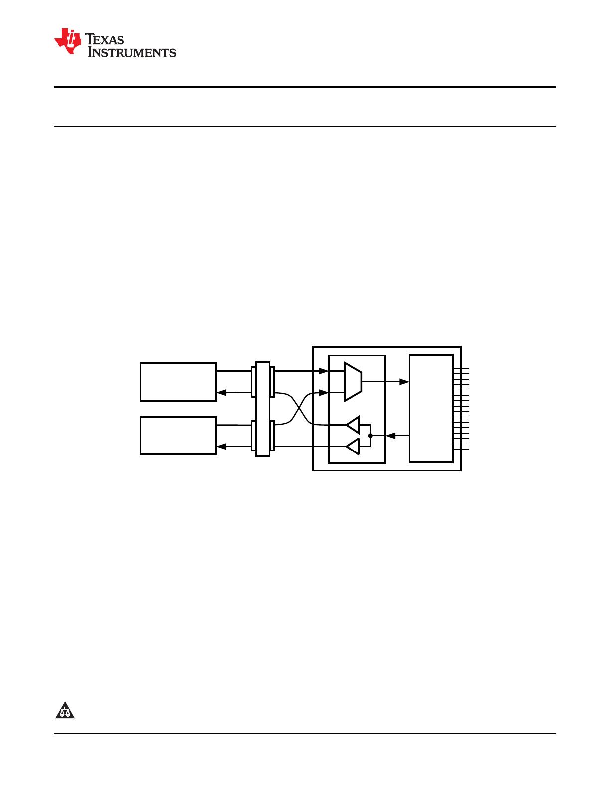
没有合适的资源?快使用搜索试试~ 我知道了~
TI-DS15MB200.pdf
5星 · 超过95%的资源 需积分: 0 2 下载量 136 浏览量
2023-02-08
23:36:05
上传
评论 4
收藏 1.01MB PDF 举报
温馨提示
试读
20页
LVDS缓冲器
资源推荐
资源详情
资源评论
Mux Buffer
Switch
Fabric A
Switch
Fabric B
FPGA
or
ASIC
Backplane or Cable
LVDS
LVDS
DS15MB200
www.ti.com
SNLS196E –NOVEMBER 2005–REVISED MARCH 2013
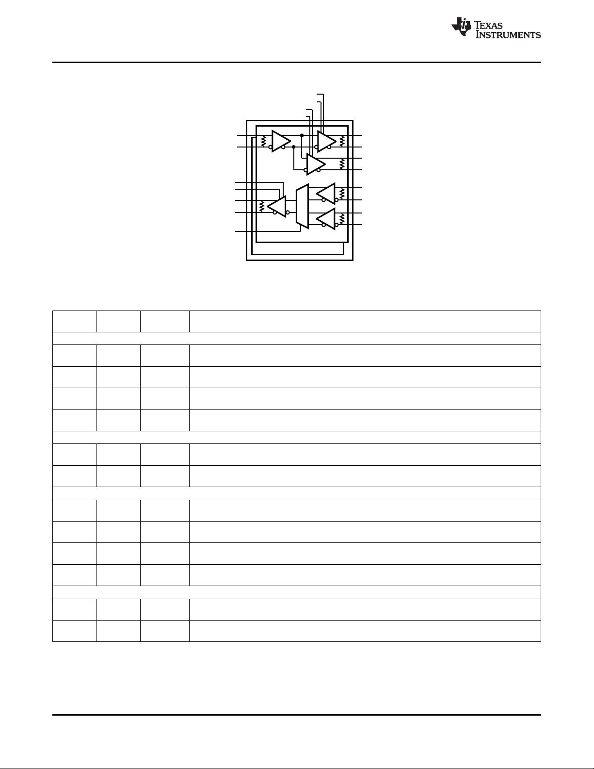
DS15MB200 Dual 1.5 Gbps 2:1/1:2 LVDS Mux/Buffer with Pre-Emphasis
Check for Samples: DS15MB200
1
FEATURES
DESCRIPTION
The DS15MB200 is a dual-port 2 to 1 multiplexer and
2
• 1.5 Gbps Data Rate Per Channel
1 to 2 repeater/buffer. High-speed data paths and
• Configurable Off/On Pre-emphasis Drives
flow-through pinout minimize internal device jitter and
Lossy Backplanes and Cables
simplify board layout, while pre-emphasis overcomes
• LVDS/BLVDS/CML/LVPECL Compatible Inputs,
ISI jitter effects from lossy backplanes and cables.
The differential inputs and outputs interface to LVDS
LVDS Compatible Outputs
or Bus LVDS signals such as those on Texas
• Low Output Skew and Jitter
Instrument's 10-, 16-, and 18-bit Bus LVDS SerDes,
• On-chip 100Ω Input and Output Termination
or to CML or LVPECL signals.
• 15 kV ESD Protection on LVDS Inputs/Outputs
The 3.3V supply, CMOS process, and robust I/O
• Hot Plug Protection
ensure high performance at low power over the entire
industrial -40 to +85°C temperature range.
• Single 3.3V Supply
• Industrial -40 to +85°C Temperature Range
• 48-pin WQFN Package
Typical Application
Figure 1.
1
Please be aware that an important notice concerning availability, standard warranty, and use in critical applications of
Texas Instruments semiconductor products and disclaimers thereto appears at the end of this data sheet.
2All trademarks are the property of their respective owners.
PRODUCTION DATA information is current as of publication date.
Copyright © 2005–2013, Texas Instruments Incorporated
Products conform to specifications per the terms of the Texas
Instruments standard warranty. Production processing does not
necessarily include testing of all parameters.
Channel 1
Channel 0
LI_0
SOA_0
SOB_0
SIA_0
SIB_0
MUX_S0
PREA_0
ENA_0
PREB_0
ENB_0
LO_0
PREL_0
ENL_0
DS15MB200
SNLS196E –NOVEMBER 2005–REVISED MARCH 2013
www.ti.com
Block Diagram
Figure 2.
PIN DESCRIPTIONS
Pin WQFN Pin
I/O, Type Description
Name Number
SWITCH SIDE DIFFERENTIAL INPUTS
SIA_0+ 30 I, LVDS Switch A-side Channel 0 inverting and non-inverting differential inputs. LVDS, Bus LVDS, CML, or
SIA_0− 29 LVPECL compatible.
SIA_1+ 19 I, LVDS Switch A-side Channel 1 inverting and non-inverting differential inputs. LVDS, Bus LVDS, CML, or
SIA_1− 20 LVPECL compatible.
SIB_0+ 28 I, LVDS Switch B-side Channel 0 inverting and non-inverting differential inputs. LVDS, Bus LVDS, CML, or
SIB_0− 27 LVPECL compatible.
SIB_1+ 21 I, LVDS Switch B-side Channel 1 inverting and non-inverting differential inputs. LVDS, Bus LVDS, CML, or
SIB_1− 22 LVPECL compatible.
LINE SIDE DIFFERENTIAL INPUTS
LI_0+ 40 I, LVDS Line-side Channel 0 inverting and non-inverting differential inputs. LVDS, Bus LVDS, CML, or
LI_0− 39 LVPECL compatible.
LI_1+ 9 I, LVDS Line-side Channel 1 inverting and non-inverting differential inputs. LVDS, Bus LVDS, CML, or
LI_1− 10 LVPECL compatible.
SWITCH SIDE DIFFERENTIAL OUTPUTS
SOA_0+ 34 O, LVDS Switch A-side Channel 0 inverting and non-inverting differential outputs. LVDS compatible
(1)(2)
.
SOA_0− 33
SOA_1+ 15 O, LVDS Switch A-side Channel 1 inverting and non-inverting differential outputs. LVDS compatible
(1)(2)
.
SOA_1− 16
SOB_0+ 32 O, LVDS Switch B-side Channel 0 inverting and non-inverting differential outputs. LVDS compatible
(1)(2)
.
SOB_0− 31
SOB_1+ 17 O, LVDS Switch B-side Channel 1 inverting and non-inverting differential outputs. LVDS compatible
(1)(2)
.
SOB_1− 18
LINE SIDE DIFFERENTIAL OUTPUTS
LO_0+ 42 O, LVDS Line-side Channel 0 inverting and non-inverting differential outputs. LVDS compatible
(1)(2)
.
LO_0− 41
LO_1+ 7 O, LVDS Line-side Channel 1 inverting and non-inverting differential outputs. LVDS compatible
(1)(2)
.
LO_1− 8
(1) For interfacing LVDS outputs to CML or LVPECL compatible inputs, refer to the applications section of this datasheet (planned).
(2) The LVDS outputs do not support a multidrop (BLVDS) environment. The LVDS output characteristics of the DS15MB200 device have
been optimized for point-to-point backplane and cable applications.
2 Submit Documentation Feedback Copyright © 2005–2013, Texas Instruments Incorporated
Product Folder Links: DS15MB200
V
DD
GND
V
DD
ENL_0
PREL_0
V
DD
LO_0+
LO_0-
LI_0+
LI_0-
MUX_S0
V
DD
48
47
46
45
44
43
42
41
40
39
38
37
ENA_1
ENB_1
SOA_1+
SOA_1-
SOB_1+
SOB_1-
SIA_1+
SIA_1-
SIB_1+
SIB_1-
PREA_1
PREB_1
13
14
15
16
17
18
19
20
21
22
23
24
V
DD
MUX_S1
LI_1-
LI_1+
LO_1-
LO-1+
V
DD
PREL_1
ENL_1
GND
V
DD
N/C
12 11 10 9 8 7 6 5 4 3 2 1
PREB_0
PREA_0
SIB_0-
SIB_0+
SIA_0-
SIA_0+
SOB_0-
SOB_0+
SOA_0-
SOA_0+
ENB_0
ENA_0
25 26 27 28 29 30 31 32 33 34 35 36
DAP
(GND)
V
DD
GND
V
DD
ENL_0
PREL_0
V
DD
LO_0+
LO_0-
LI_0+
LI_0-
MUX_S0
V
DD
ENA_1
ENB_1
SOA_1+
SOA_1-
SOB_1+
SOB_1-
SIA_1+
SIA_1-
SIB_1+
SIB_1-
PREA_1
PREB_1
V
DD
MUX_S1
LI_1-
LI_1+
LO_1-
LO-1+
V
DD
PREL_1
ENL_1
GND
V
DD
N/C
PREB_0
PREA_0
SIB_0-
SIB_0+
SIA_0-
SIA_0+
SOB_0-
SOB_0+
SOA_0-
SOA_0+
ENB_0
ENA_0
Channel 0
Channel 1
DS15MB200
www.ti.com
SNLS196E –NOVEMBER 2005–REVISED MARCH 2013
PIN DESCRIPTIONS (continued)
Pin WQFN Pin
I/O, Type Description
Name Number
DIGITAL CONTROL INTERFACE
MUX_S0 38 I, LVTTL Mux Select Control Inputs (per channel) to select which Switch-side input, A or B, is passed through
MUX_S1 11 to the Line-side.
PREA_0 26 I, LVTTL Output pre-emphasis control for Switch-side outputs. Each output driver on the Switch A-side and B-
PREA_1 23 side has a separate pin to control the pre-emphasis on or off.
PREB_0 25
PREB_1 24
PREL_0 44 I, LVTTL Output pre-emphasis control for Line-side outputs. Each output driver on the Line A-side and B-side
PREL_1 5 has a separate pin to control the pre-emphasis on or off.
ENA_0 36 I, LVTTL Output Enable Control for Switch A-side and B-side outputs. Each output driver on the A-side and
ENA_1 13 B-side has a separate enable pin.
ENB_0 35
ENB_1 14
ENL_0 45 I, LVTTL Output Enable Control for The Line-side outputs. Each output driver on the Line-side has a separate
ENL_1 4 enable pin.
POWER
V
DD
2, 6, 12, I, Power V
DD
= 3.3V ±0.3V.
37, 43, 46,
48
GND 3, 47
(3)
I, Power Ground reference for LVDS and CMOS circuitry.
For the WQFN package, the DAP is used as the primary GND connection to the device. The DAP is
the exposed metal contact at the bottom of the WQFN-48 package. It should be connected to the
ground plane with at least 4 vias for optimal AC and thermal performance.
(3) Note that the DAP on the backside of the WQFN package is the primary GND connection for the device when using the WQFN
package.
Connection Diagrams
Figure 3. WQFN Top View Figure 4. Directional Signal Paths Top View
DAP = GND (Refer to pin names for signal polarity)
Copyright © 2005–2013, Texas Instruments Incorporated Submit Documentation Feedback 3
Product Folder Links: DS15MB200
DS15MB200
SNLS196E –NOVEMBER 2005–REVISED MARCH 2013
www.ti.com
Output Characteristics
The output characteristics of the DS15MB200 have been optimized for point-to-point backplane and cable
applications, and are not intended for multipoint or multidrop signaling.
A 100Ω output (source) termination resistor is incorporated in the device to eliminate the need for an external
resistor, providing excellent drive characteristics by locating the source termination as close to the output as
physically possible.
Pre-Emphasis Controls
The pre-emphasis is used to compensate for long or lossy transmission media. Separate pins are provided for
each output to minimize power consumption. Pre-emphasis is programmable to be off or on per the Pre-
emphasis Control Table.
PREx_n
(1)
Output Pre-Emphasis
0 0%
1 100%
(1) Applies to PREA_0, PREA_1, PREB_0, PREB_1, PREL_0, PREL_1
Multiplexer Truth Table
(2)(3)
Data Inputs Control Inputs Output
SIA_0 SIB_0 MUX_S0 ENL_0 LO_0
X valid 0 1 SIB_0
valid X 1 1 SIA_0
X X X 0 Z
(2) Same functionality for channel 1
(3) X = Don't Care
Z = High Impedance (TRI-STATE)
Repeater/Buffer Truth Table
(1)(2)
Data Input Control Inputs Outputs
LI_0 ENA_0 ENB_0 SOA_0 SOB_0
X 0 0 Z Z
valid 0 1 Z LI_0
valid 1 0 LI_0 Z
valid 1 1 LI_0 LI_0
(1) Same functionality for channel 1
(2) X = Don't Care
Z = High Impedance (TRI-STATE)
These devices have limited built-in ESD protection. The leads should be shorted together or the device placed in conductive foam
during storage or handling to prevent electrostatic damage to the MOS gates.
4 Submit Documentation Feedback Copyright © 2005–2013, Texas Instruments Incorporated
Product Folder Links: DS15MB200
剩余19页未读,继续阅读
资源评论
- qq_335607272023-02-15#完美解决问题 #运行顺畅 #内容详尽 #全网独家 #注释完整
- m0_745259962023-02-15#完美解决问题 #运行顺畅 #内容详尽 #全网独家 #注释完整
不觉明了
- 粉丝: 3242
- 资源: 5614
上传资源 快速赚钱
- 我的内容管理 展开
- 我的资源 快来上传第一个资源
- 我的收益 登录查看自己的收益
- 我的积分 登录查看自己的积分
- 我的C币 登录后查看C币余额
- 我的收藏
- 我的下载
- 下载帮助
最新资源
- delphi语言入门教程+培训大纲
- 华为HCIA-WLAN 3.0 课程视频(30 WLAN安全配置.mp4)
- 华为HCIA-WLAN 3.0 课程视频(29 WLAN网络准入控制.mp4)
- 华为HCIA-WLAN 3.0 课程视频(28 WLAN数据安全.mp4)
- 华为HCIA-WLAN 3.0 课程视频(27 WLAN接入安全.mp4)
- php语言入门教程-自学笔记
- 华为HCIA-WLAN 3.0 课程视频(26 WLAN安全威胁与防御.mp4)
- 基于Python+OpenCV的指纹识别系统+源代码+结果截图(高分项目).zip
- mysql和navicat安装包
- Val-EdgeMapVal-EdgeMap
资源上传下载、课程学习等过程中有任何疑问或建议,欢迎提出宝贵意见哦~我们会及时处理!
点击此处反馈
安全验证
文档复制为VIP权益,开通VIP直接复制
信息提交成功