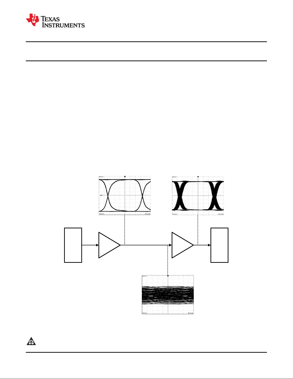
没有合适的资源?快使用搜索试试~ 我知道了~
TI-DS15BA101.pdf
![star](https://csdnimg.cn/release/downloadcmsfe/public/img/star.98a08eaa.png)
温馨提示
![preview](https://dl-preview.csdnimg.cn/87429838/0001-284ca75c99e71ef70065758d5340bb6b_thumbnail.jpeg)
![preview-icon](https://csdnimg.cn/release/downloadcmsfe/public/img/scale.ab9e0183.png)
试读
15页
LVDS缓冲器
资源推荐
资源详情
资源评论
![pdf](https://img-home.csdnimg.cn/images/20210720083512.png)
![](https://csdnimg.cn/release/download_crawler_static/87429838/bg1.jpg)
Serializer
Deserializer
DS15BA101 DS15EA101
CML
LVPECL
LVDS
150 Mbps
to
1.5 Gbps
100-ohm Differential Cable
(i.e. CAT5e/6/7, Twinax)
50-ohm Coaxial Cable
(i.e. Belden 9914)
Max Cable Loss ~ 35 dB @ 750 MHz
DS15BA101
www.ti.com
SNLS234J –OCTOBER 2006–REVISED APRIL 2013
DS15BA101 1.5 Gbps Differential Buffer with Adjustable Output Voltage
Check for Samples: DS15BA101
1
FEATURES
DESCRIPTION
The DS15BA101 is a high-speed differential buffer for
2
• Data Rates from DC to 1.5+ Gbps
cable driving, level translation, signal buffering, and
• Differential or Single-ended Input
signal repeating applications. Its fully differential
• Adjustable Output Amplitude
signal path ensures exceptional signal integrity and
noise immunity and it drives both differential and
• Single 3.3V Supply
single-ended transmission lines at data rates in
• Industrial -40°C to +85°C Temperature
excess of 1.5 Gbps.
• Low Power: 150 mW (typ) at 1.5 Gbps
Output voltage amplitude is adjustable via a single
• Space-saving 3 x 3 mm WSON-8 Package
external resistor for level translation and cable driving
applications into 50-ohm single-ended and 100-ohm
APPLICATIONS
differential mode impedances.
• Cable Extension Applications
The DS15BA101 is powered from a single 3.3V
• Level Translation
supply and consumes 150 mW (typ) at 1.5 Gbps. It
operates over the full −40°C to +85°C industrial
• Signal Buffering and Repeating
temperature range and is available in a space saving
• Security Cameras
3x3 mm WSON-8 package.
Typical Application
1
Please be aware that an important notice concerning availability, standard warranty, and use in critical applications of
Texas Instruments semiconductor products and disclaimers thereto appears at the end of this data sheet.
2All trademarks are the property of their respective owners.
PRODUCTION DATA information is current as of publication date.
Copyright © 2006–2013, Texas Instruments Incorporated
Products conform to specifications per the terms of the Texas
Instruments standard warranty. Production processing does not
necessarily include testing of all parameters.
![](https://csdnimg.cn/release/download_crawler_static/87429838/bg2.jpg)
DS15BA101
SNLS234J –OCTOBER 2006–REVISED APRIL 2013
www.ti.com
These devices have limited built-in ESD protection. The leads should be shorted together or the device placed in conductive foam
during storage or handling to prevent electrostatic damage to the MOS gates.
Absolute Maximum Ratings
(1)
Supply Voltage −0.5V to 3.6V
Input Voltage (all inputs) −0.3V to V
CC
+0.3V
Output Current 28 mA
Storage Temperature Range −65°C to +150°C
Junction Temperature +150°C
Lead Temperature
(Soldering 4 Sec) +260°C
θ
JA
WSON-8 +90.7°C/W
Package Thermal Resistance
θ
JC
WSON-8 +41.2°C/W
ESD Rating (HBM) 5 kV
ESD Rating (MM) 250V
(1) "Absolute Maximum Ratings" are those parameter values beyond which the life and operation of the device cannot be ensured. The
stating herein of these maximums shall not be construed to imply that the device can or should be operated at or beyond these values.
The table of "Electrical Characteristics" specifies acceptable device operating conditions.
Recommended Operating Conditions
Supply Voltage (VCC – GND): 3.3V ±5%
Operating Free Air Temperature (T
A
)
DS15BA101SD −40°C to +85°C
DC Electrical Characteristics
Over Supply Voltage and Operating Temperature ranges, unless otherwise specified.
(1)(2)
Symbol Parameter Conditions Reference Min Typ Max Units
V
ICM
Input Common Mode Voltage See Note
(3)
IN+, IN- V
CC
–
0.8 V
V
ID
/2
V
ID
Differential Input Voltage Swing 100 2000 mV
P−P
V
OS
Output Common Mode Voltage OUT+, OUT- V
CC
–
V
V
OUT
/2
V
OUT
Output Voltage Single-ended, 25Ω load
400 mV
P-P
R
VO
= 953Ω 1%,
Single-ended, 25Ω load
800 mV
P-P
R
VO
= 487Ω 1%,
I
CC
Supply Current See Note
(4)
45 49 mA
(1) Current flow into device pins is defined as positive. Current flow out of device pins is defined as negative. All voltages are stated
referenced to GND.
(2) Typical values are stated for V
CC
= +3.3V and T
A
= +25°C.
(3) Specification is ensured by characterization.
(4) Maximum I
CC
is measured at V
CC
= +3.465V and T
A
= +70°C.
2 Submit Documentation Feedback Copyright © 2006–2013, Texas Instruments Incorporated
Product Folder Links: DS15BA101
![](https://csdnimg.cn/release/download_crawler_static/87429838/bg3.jpg)
IN+
IN-
GND
R
VO
OUT+
OUT-
GND
VCC
1
2
3
4
8
6
5
7
(GND)
DAP
DS15BA101
www.ti.com
SNLS234J –OCTOBER 2006–REVISED APRIL 2013
AC Electrical Characteristics
Over Supply Voltage and Operating Temperature ranges, unless otherwise specified
(1)
.
Symbol Parameter Conditions Reference Min Typ Max Units
DR
MAX
Maximum Data Rate See Note
(2)
IN+, IN- 1.5 2.0 Gbps
t
LHT
Output Low to High Transition 20% – 80%
(3)
OUT+, OUT-
120 220 ps
Time
t
HLT
Output High to Low Transition
120 220 ps
Time
t
PLHD
Propagation Low to High Delay See Note
(2)
0.95 1.10 1.35 ns
t
PHLD
Propagation High to Low Delay See Note
(2)
0.95 1.10 1.35 ns
t
TJ
Total Jitter 1.5 Gbps 26 ps
P-P
(1) Typical values are stated for V
CC
= +3.3V and T
A
= +25°C.
(2) Specification is ensured by characterization.
(3) Specification is ensured by characterization and verified by test.
CONNECTION DIAGRAM
Figure 1. 8-Pad WSON
See NGQ Package
PIN DESCRIPTIONS
Pin # Name Description
1 IN+ Non-inverting input pin.
2 IN- Inverting input pin.
3 GND Circuit common (ground reference).
4 R
VO
Output voltage amplitude control. Connect a resistor to V
CC
to set output voltage.
5 V
CC
Positive power supply (+3.3V).
6 GND Circuit common (ground reference).
7 OUT- Inverting output pin.
8 OUT+ Non-inverting output pin.
Copyright © 2006–2013, Texas Instruments Incorporated Submit Documentation Feedback 3
Product Folder Links: DS15BA101
剩余14页未读,继续阅读
资源评论
![avatar-default](https://csdnimg.cn/release/downloadcmsfe/public/img/lazyLogo2.1882d7f4.png)
- qq_335607272023-02-15#完美解决问题 #运行顺畅 #内容详尽 #全网独家 #注释完整
- m0_745259962023-02-15#完美解决问题 #运行顺畅 #内容详尽 #全网独家 #注释完整
![avatar](https://profile-avatar.csdnimg.cn/107303f5121d47e49d12d0a9ae68af10_weixin_54787054.jpg!1)
不觉明了
- 粉丝: 3236
- 资源: 5614
上传资源 快速赚钱
我的内容管理 展开
我的资源 快来上传第一个资源
我的收益
登录查看自己的收益我的积分 登录查看自己的积分
我的C币 登录后查看C币余额
我的收藏
我的下载
下载帮助
![voice](https://csdnimg.cn/release/downloadcmsfe/public/img/voice.245cc511.png)
![center-task](https://csdnimg.cn/release/downloadcmsfe/public/img/center-task.c2eda91a.png)
安全验证
文档复制为VIP权益,开通VIP直接复制
![dialog-icon](https://csdnimg.cn/release/downloadcmsfe/public/img/green-success.6a4acb44.png)