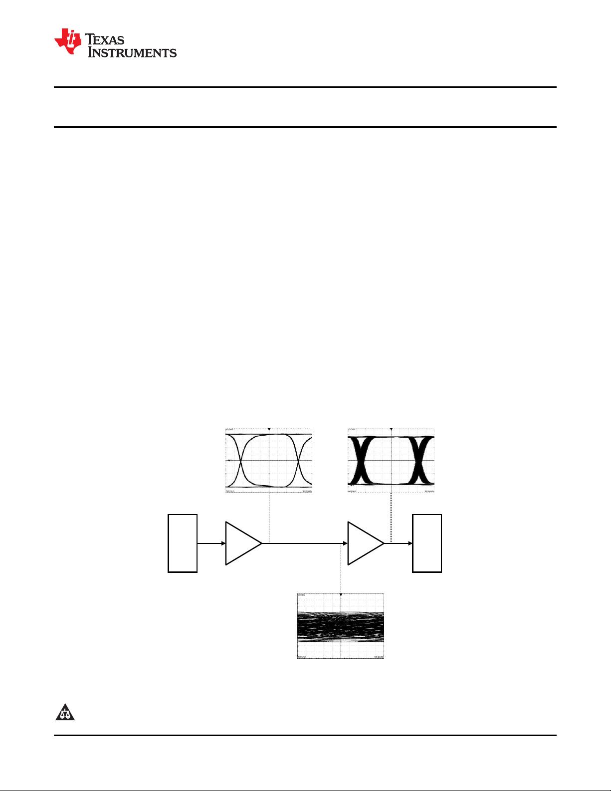
没有合适的资源?快使用搜索试试~ 我知道了~
TI-DS15EA101.pdf
5星 · 超过95%的资源 需积分: 12 1 下载量 47 浏览量
2022-12-04
00:18:15
上传
评论 4
收藏 1.02MB PDF 举报
温馨提示
试读
19页
TI-DS15EA101.pdf
资源推荐
资源详情
资源评论
Serializer
Deserializer
DS15BA101 DS15EA101
CML
LVPECL
LVDS
150 Mbps
to
1.5 Gbps
100-ohm Differential Cable
(i.e. CAT5e/6/7, Twinax)
50-ohm Coaxial Cable
(i.e. Belden 9914)
Max Cable Loss ~ 35 dB @ 750 MHz
DS15EA101
www.ti.com
SNLS235H –SEPTEMBER 2006–REVISED APRIL 2013
DS15EA101 0.15 to 1.5 Gbps Adaptive Cable Equalizer with LOS Detection
Check for Samples: DS15EA101
1
FEATURES
DESCRIPTION
The DS15EA101 is an adaptive equalizer optimized
2
• Automatic Equalization of Coaxial, Twin-Ax
for equalizing data transmitted over copper cables.
and Twisted Pair Cables
The DS15EA101 operates over a wide range of data
• High Data Rates: 150 Mbps to 1.5+ Gbps
rates from 150 Mbps to 1.5+ Gbps and automatically
• Up to 35 dB of Boost at 750 MHz
adapts to equalize any cable length from zero meters
to lengths that attenuate the signal by 35 dB at 750
• LOS Detection and Output Enable
MHz.
• Single-Ended or Differential Input
The DS15EA101 allows either single-ended or
• 50Ω Differential Outputs
differential input drive. This enables equalization of
• Low Power Operation, 210 mW (typ) at 1.5
coaxial cables as well as differential twin-ax and
Gbps
twisted pair cables.
• Industrial -40°C to +85°C Temperature
Additional features include an LOS output and an
• Space-Saving 4 x 4 mm WQFN-16 Package
output enable which, when tied together, disable the
output when no signal is present.
APPLICATIONS
The DS15EA101 is powered from a single 3.3V
• Cable Extention Applications
supply and consumes 210 mW at 1.5 Gbps. It
operates over the full −40°C to +85°C industrial
• Security Cameras
temperature range and is available in a space saving
• Remote LCDs and LED Panels
4 x 4 mm WQFN-16 package which allows for high
• Data Recovery Equalization
density placement of components in multi-channel
applications.
Typical Application
1
Please be aware that an important notice concerning availability, standard warranty, and use in critical applications of
Texas Instruments semiconductor products and disclaimers thereto appears at the end of this data sheet.
2All trademarks are the property of their respective owners.
PRODUCTION DATA information is current as of publication date.
Copyright © 2006–2013, Texas Instruments Incorporated
Products conform to specifications per the terms of the Texas
Instruments standard warranty. Production processing does not
necessarily include testing of all parameters.
DS15EA101
SNLS235H –SEPTEMBER 2006–REVISED APRIL 2013
www.ti.com
These devices have limited built-in ESD protection. The leads should be shorted together or the device placed in conductive foam
during storage or handling to prevent electrostatic damage to the MOS gates.
Absolute Maximum Ratings
(1)
Supply Voltage −0.5V to 3.6V
Input Voltage (all inputs) −0.3V to V
CC
+0.3V
Storage Temperature Range −65°C to +150°C
Junction Temperature +150°C
Lead Temperature
(Soldering 4 Sec) +260°C
Package Thermal Resistance
θ
JA
RGH0016A +42.1°C/W
θ
JC
RGH0016A +8.2°C/W
ESD Rating (HBM) 8 kV
ESD Rating (MM) 250V
(1) "Absolute Maximum Ratings" are those parameter values beyond which the life and operation of the device cannot be ensured. The
stating herein of these maximums shall not be construed to imply that the device can or should be operated at or beyond these values.
The table of Electrical Characteristics specifies acceptable device operating conditions.
Recommended Operating Conditions
Supply Voltage (VCC ) 3.3V ±5%
Input Coupling Capacitance 1.0 µF
Loop Capacitor (Connected between
CAP+ and CAP-) 1.0 µF
Operating Free Air Temperature (T
A
) -40°C to +85°C
DC Electrical Characteristics
Over Supply Voltage and Operating Temperature ranges, unless otherwise specified
(1) (2)
.
Symbol Parameter Conditions Reference Min Typ Max Units
V
CM
Input Common Mode Voltage IN+, IN- 1.9 V
V
IN
Input Voltage
(3)(4)
950 mV
P-P
V
CC
–
V
OS
Output Common Mode Voltage V
V
OUT
/2
OUT+, OUT-
V
OUT
Output Voltage Swing 50Ω load, differential 750 mV
P-P
V
LOS
LOS Output Voltage Valid signal not present LOS 2.6 V
Valid signal present 0.4 V
V
IN(EN)
EN Input Voltage Min to disable outputs EN 3.0 V
Max to enable outputs 0.8 V
I
CC
Supply Current
(5)
63 77 mA
(1) Current flow into device pins is defined as positive. Current flow out of device pins is defined as negative. All voltages are stated
referenced to 0 volts.
(2) Typical values are stated for V
CC
= +3.3V and T
A
= +25°C.
(3) Specification is ensured by characterization.
(4) The maximum input voltage amplitude assumes a DC-balanced signal.
(5) Supply current depends on the amount of cable being equalized. The current is highest for short cable and decreases as the cable
length is increased.
2 Submit Documentation Feedback Copyright © 2006–2013, Texas Instruments Incorporated
Product Folder Links: DS15EA101
GND
IN+
IN-
GND
GND
OUT+
OUT-
GND
1
2
3
4
12
10
9
11
(GND)
DAP
CAP+
CAP-
GND
GND
5
6
7
8
VCC
LOS
EN
VCC
16
14
13
15
DS15EA101
www.ti.com
SNLS235H –SEPTEMBER 2006–REVISED APRIL 2013
AC Electrical Characteristics
Over Supply Voltage and Operating Temperature ranges, unless otherwise specified
(1)
.
Symbol Parameter Conditions Reference Min Typ Max Units
BR
IN
Input Data Rate IN+, IN- 150 1500 Mbps
t
TRJ
Total Residual Jitter @ BER-12 1.5 Gbps
(2)
25m CAT5e (Belden 1700A), 0.25 UI
(1)
1.0 Gbps
50m CAT5e (Belden 1700A), 0.25 UI
(1)
0.5 Gbps
100m CAT5e (Belden 1700A), 0.25 UI
(1)
1.5 Gbps
50m CAT7 (Siemon Tera), 0.25 UI
(1)
1.5 Gbps
75m CAT7 (Siemon Tera), 0.30 UI
(1)
1.0 Gbps
100m CAT7 (Siemon Tera), 0.40 UI
(1)
1.5 Gbps
200m Belden 9914, 0.25 UI
(1)
tTLH Transition Time from Low to 20% – 80%,
(3)
OUT+, OUT-
100 220 ps
High
tTHL Transition Time from High to 20% – 80%,
(3)
100 220 ps
Low
R
OUT
Output Resistance single-ended,
(4)
50 Ω
(1) Typical values are stated for V
CC
= +3.3V and T
A
= +25°C.
(2) The total residual jitter at BER-12 was calculated as DJ+14.1xRJ, where DJ is deterministic jitter and RJ is random jitter. The jitter is
expressed as a portion of a unit interval (UI). One UI is a reciprocal of a bit rate (or data rate). For example, a 1.5 Gbps (gigabit per
second) signal has 1 / (1.5 Gb/s) = 666.67 ps (picosecond) unit interval. A 0.25 UI jitter is equivalent to 0.25 x 666.67 ps = 166.67 ps.
(3) Specification is ensured by characterization.
(4) Specification is ensured by design.
CONNECTION DIAGRAM
16-Pad WQFN
Package Number RGH0016A
Copyright © 2006–2013, Texas Instruments Incorporated Submit Documentation Feedback 3
Product Folder Links: DS15EA101
DS15EA101
SNLS235H –SEPTEMBER 2006–REVISED APRIL 2013
www.ti.com
PIN DESCRIPTIONS
Pin # Name Description
1 GND Ground pin.
2 IN+ Non-inverting input pin.
3 IN- Inverting input pin.
4 GND Ground pin.
5 CAP+ Loop filter positive pin.
6 CAP- Loop filter negative pin.
7 GND Ground pin.
8 GND Ground pin.
9 GND Ground pin.
10 OUT- Inverting output pin.
11 OUT+ Non-inverting output pin.
12 GND Ground pin.
13 VCC Power supply pin.
14 EN Output enable pin.
15 LOS Los of signal circuitry output pin.
16 VCC Power supply pin.
4 Submit Documentation Feedback Copyright © 2006–2013, Texas Instruments Incorporated
Product Folder Links: DS15EA101
剩余18页未读,继续阅读
资源评论
- qq_335607272022-12-04#完美解决问题 #运行顺畅 #内容详尽 #全网独家 #注释完整
不觉明了
- 粉丝: 3164
- 资源: 5429
上传资源 快速赚钱
- 我的内容管理 展开
- 我的资源 快来上传第一个资源
- 我的收益 登录查看自己的收益
- 我的积分 登录查看自己的积分
- 我的C币 登录后查看C币余额
- 我的收藏
- 我的下载
- 下载帮助
安全验证
文档复制为VIP权益,开通VIP直接复制
信息提交成功