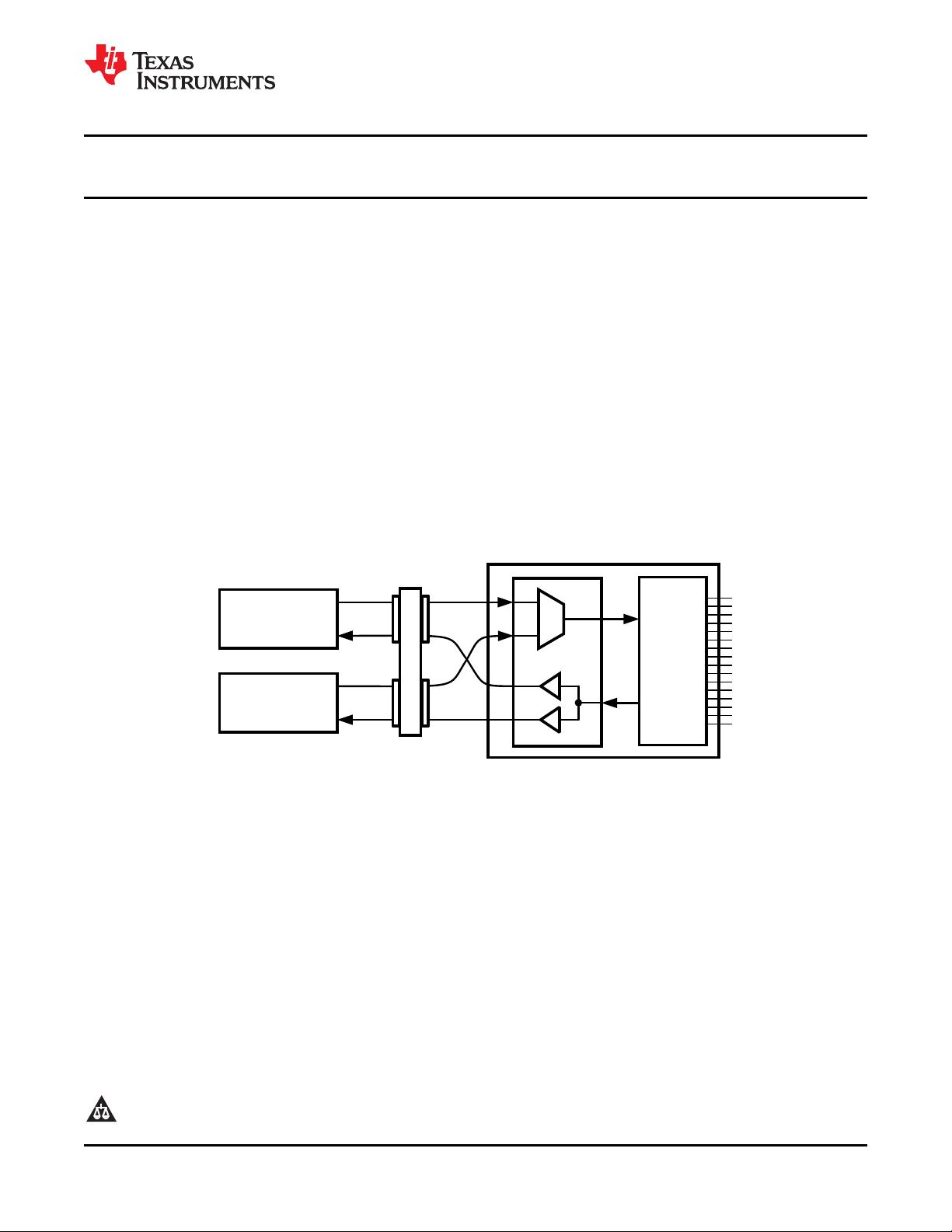
没有合适的资源?快使用搜索试试~ 我知道了~
TI-SCAN15MB200.pdf
5星 · 超过95%的资源 需积分: 0 3 下载量 105 浏览量
2023-02-08
23:33:16
上传
评论 4
收藏 989KB PDF 举报
温馨提示
试读
22页
LVDS缓冲器
资源推荐
资源详情
资源评论
Mux Buffer
Switch
Fabric A
Switch
Fabric B
FPGA
or
ASIC
Backplane or Cable
LVDS
LVDS
SCAN15MB200
www.ti.com
SNLS188E –NOVEMBER 2005–REVISED APRIL 2013
Dual 1.5 Gbps 2:1/1:2 LVDS Mux/Buffer with Pre-Emphasis and IEEE 1149.6
Check for Samples: SCAN15MB200
1
FEATURES
DESCRIPTION
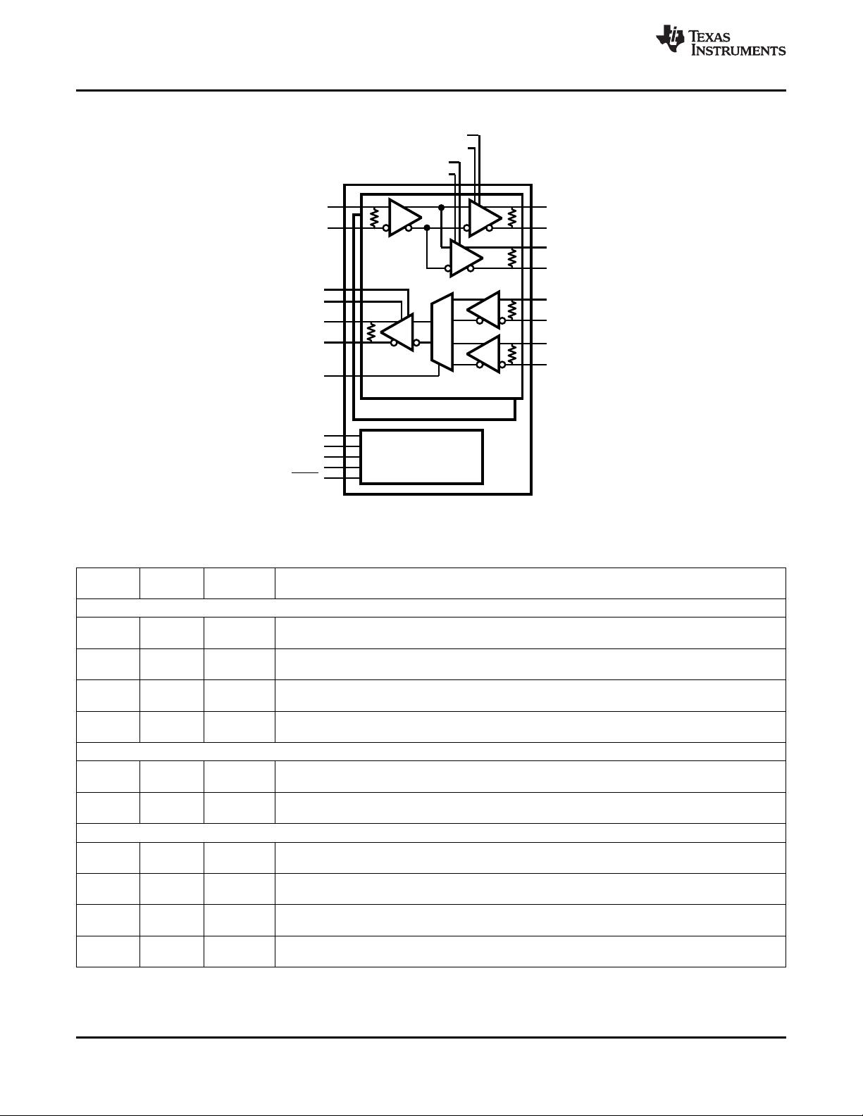
The SCAN15MB200 is a dual-port 2 to 1 multiplexer
2
• 1.5 Gbps Data Rate Per Channel
and 1 to 2 repeater/buffer. High-speed data paths
• Configurable Off/On Pre-emphasis Drives
and flow-through pinout minimize internal device jitter
Lossy Backplanes and Cables
and simplify board layout, while pre-emphasis
• LVDS/BLVDS/CML/LVPECL Compatible Inputs,
overcomes ISI jitter effects from lossy backplanes
and cables. The differential inputs and outputs
LVDS Compatible Outputs
interface to LVDS or Bus LVDS signals such as those
• Low Output Skew and Jitter
on TI's 10-, 16-, and 18- bit Bus LVDS SerDes, or to
• On-chip 100Ω Input and Output Termination
CML or LVPECL signals.
• IEEE 1149.1 and 1149.6 Compliant
Integrated IEEE 1149.1 (JTAG) and 1149.6 circuitry
• 15 kV ESD Protection on LVDS Inputs/Outputs
supports testability of both single-ended
LVTTL/CMOS and high-speed differential PCB
• Hot Plug Protection
interconnects. The 3.3V supply, CMOS process, and
• Single 3.3V Supply
robust I/O ensure high performance at low power
• Industrial -40 to +85°C Temperature Range
over the entire industrial -40 to +85°C temperature
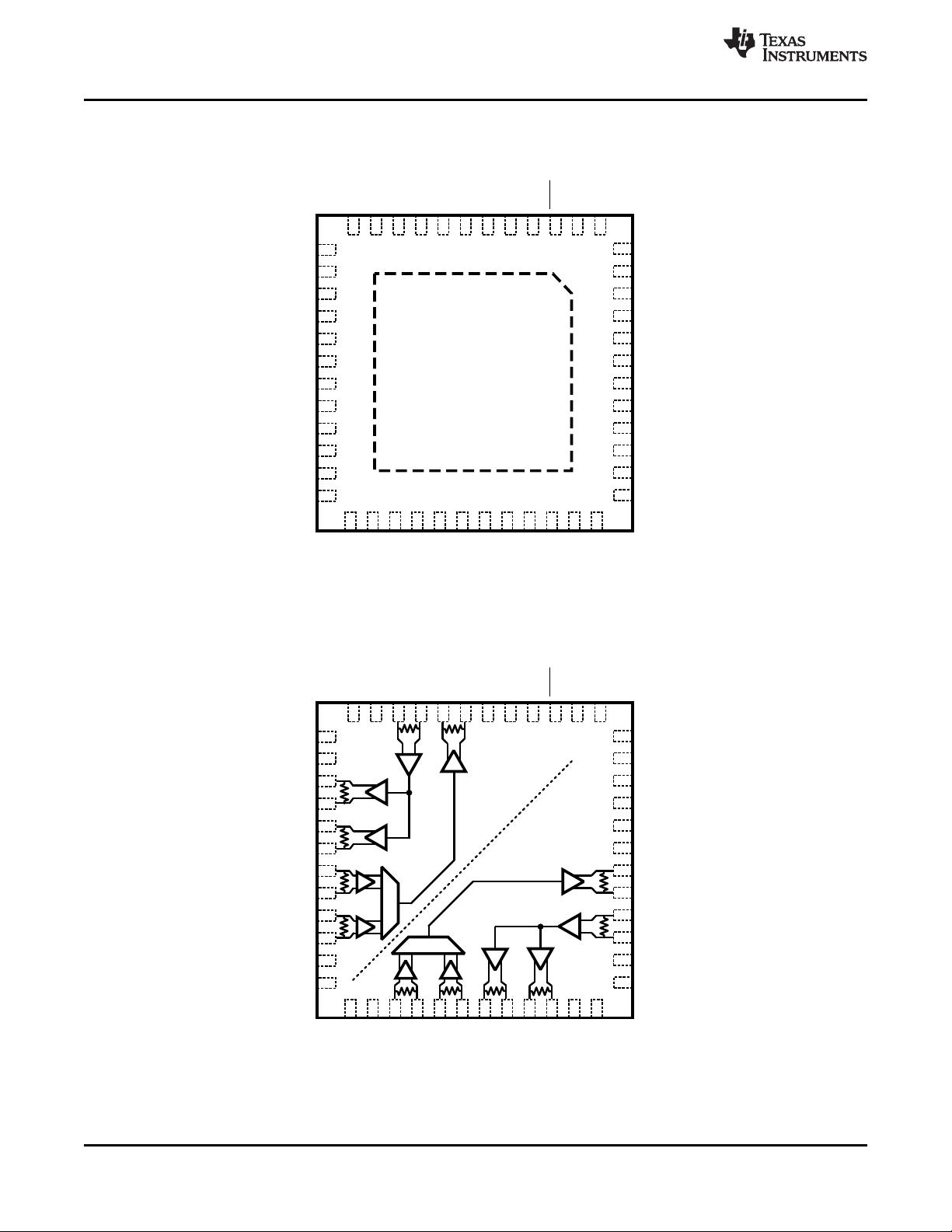
• 48-Pin WQFN Package
range.
Typical Application
1
Please be aware that an important notice concerning availability, standard warranty, and use in critical applications of
Texas Instruments semiconductor products and disclaimers thereto appears at the end of this data sheet.
2All trademarks are the property of their respective owners.
PRODUCTION DATA information is current as of publication date.
Copyright © 2005–2013, Texas Instruments Incorporated
Products conform to specifications per the terms of the Texas
Instruments standard warranty. Production processing does not
necessarily include testing of all parameters.
Channel 1
LI_0
SOA_0
SOB_0
SIA_0
SIB_0
MUX_S0
PREA_0
ENA_0
PREB_0
ENB_0
Channel 0
LO_0
PREL_0
IEEE 1149.1 (JTAG)
Test Access Port,
1149.6, Fault Insertion
TDI
TDO
TCK
TMS
TRST
ENL_0
SCAN15MB200
SNLS188E –NOVEMBER 2005–REVISED APRIL 2013
www.ti.com
Block Diagram
Figure 1. SCAN15MB200 Block Diagram
Pin Descriptions
Pin WQFN Pin
I/O, Type Description
Name Number
SWITCH SIDE DIFFERENTIAL INPUTS
SIA_0+ 30 I, LVDS Switch A-side Channel 0 inverting and non-inverting differential inputs. LVDS, Bus LVDS, CML, or
SIA_0− 29 LVPECL compatible.
SIA_1+ 19 I, LVDS Switch A-side Channel 1 inverting and non-inverting differential inputs. LVDS, Bus LVDS, CML, or
SIA_1− 20 LVPECL compatible.
SIB_0+ 28 I, LVDS Switch B-side Channel 0 inverting and non-inverting differential inputs. LVDS, Bus LVDS, CML, or
SIB_0− 27 LVPECL compatible.
SIB_1+ 21 I, LVDS Switch B-side Channel 1 inverting and non-inverting differential inputs. LVDS, Bus LVDS, CML, or
SIB_1− 22 LVPECL compatible.
LINE SIDE DIFFERENTIAL INPUTS
LI_0+ 40 I, LVDS Line-side Channel 0 inverting and non-inverting differential inputs. LVDS, Bus LVDS, CML, or
LI_0− 39 LVPECL compatible.
LI_1+ 9 I, LVDS Line-side Channel 1 inverting and non-inverting differential inputs. LVDS, Bus LVDS, CML, or
LI_1− 10 LVPECL compatible.
SWITCH SIDE DIFFERENTIAL OUTPUTS
SOA_0+ 34 O, LVDS Switch A-side Channel 0 inverting and non-inverting differential outputs. LVDS compatible
(1) (2)
.
SOA_0− 33
SOA_1+ 15 O, LVDS Switch A-side Channel 1 inverting and non-inverting differential outputs. LVDS compatible
(1) (2)
.
SOA_1− 16
SOB_0+ 32 O, LVDS Switch B-side Channel 0 inverting and non-inverting differential outputs. LVDS compatible
(1) (2)
.
SOB_0− 31
SOB_1+ 17 O, LVDS Switch B-side Channel 1 inverting and non-inverting differential outputs. LVDS compatible
(1) (2)
.
SOB_1− 18
(1) For interfacing LVDS outputs to CML or LVPECL compatible inputs, refer to the applications section of this datasheet (planned).
(2) The LVDS outputs do not support a multidrop (BLVDS) environment. The LVDS output characteristics of the SCAN15MB200 device
have been optimized for point-to-point backplane and cable applications.
2 Submit Documentation Feedback Copyright © 2005–2013, Texas Instruments Incorporated
Product Folder Links: SCAN15MB200
SCAN15MB200
www.ti.com
SNLS188E –NOVEMBER 2005–REVISED APRIL 2013
Pin Descriptions (continued)
Pin WQFN Pin
I/O, Type Description
Name Number
LINE SIDE DIFFERENTIAL OUTPUTS
LO_0+ 42 O, LVDS Line-side Channel 0 inverting and non-inverting differential outputs. LVDS compatible
(3) (4)
.
LO_0− 41
LO_1+ 7 O, LVDS Line-side Channel 1 inverting and non-inverting differential outputs. LVDS compatible
(3) (4)
.
LO_1− 8
DIGITAL CONTROL INTERFACE
MUX_S0 38 I, LVTTL Mux Select Control Inputs (per channel) to select which Switch-side input, A or B, is passed through
MUX_S1 11 to the Line-side.
PREA_0 26 I, LVTTL Output pre-emphasis control for Switch-side outputs. Each output driver on the Switch A-side and B-
PREA_1 23 side has a separate pin to control the pre-emphasis on or off.
PREB_0 25
PREB_1 24
PREL_0 44 I, LVTTL Output pre-emphasis control for Line-side outputs. Each output driver on the Line A-side and B-side
PREL_1 5 has a separate pin to control the pre-emphasis on or off.
ENA_0 36 I, LVTTL Output Enable Control for Switch A-side and B-side outputs. Each output driver on the A-side and
ENA_1 13 B-side has a separate enable pin.
ENB_0 35
ENB_1 14
ENL_0 45 I, LVTTL Output Enable Control for The Line-side outputs. Each output driver on the Line-side has a separate
ENL_1 4 enable pin.
TDI 2 I, LVTTL Test Data Input to support IEEE 1149.1 features
TDO 1 O, LVTTL Test Data Output to support IEEE 1149.1 features
TMS 46 I, LVTTL Test Mode Select to support IEEE 1149.1 features
TCK 47 I, LVTTL Test Clock to support IEEE 1149.1 features
TRST 3 I, LVTTL Test Reset to support IEEE 1149.1 features
POWER
V
DD
6, 12, 37, I, Power V
DD
= 3.3V ±0.3V.
43, 48
GND See
(5)
I, Power Ground reference for LVDS and CMOS circuitry.
For the WQFN package, the DAP is used as the primary GND connection to the device. The DAP is
the exposed metal contact at the bottom of the WQFN-48 package. It should be connected to the
ground plane with at least 4 vias for optimal AC and thermal performance.
(3) For interfacing LVDS outputs to CML or LVPECL compatible inputs, refer to the applications section of this datasheet (planned).
(4) The LVDS outputs do not support a multidrop (BLVDS) environment. The LVDS output characteristics of the SCAN15MB200 device
have been optimized for point-to-point backplane and cable applications.
(5) Note that the DAP on the backside of the WQFN package is the primary GND connection for the device when using the WQFN
package.
Copyright © 2005–2013, Texas Instruments Incorporated Submit Documentation Feedback 3
Product Folder Links: SCAN15MB200
V
DD
TCK
TMS
ENL_0
PREL_0
V
DD
LO_0+
LO_0-
LI_0+
LI_0-
MUX_S0
V
DD
ENA_1
ENB_1
SOA_1+
SOA_1-
SOB_1+
SOB_1-
SIA_1+
SIA_1-
SIB_1+
SIB_1-
PREA_1
PREB_1
V
DD
MUX_S1
LI_1-
LI_1+
LO_1-
LO-1+
V
DD
PREL_1
ENL_1
TRST
TDI
TDO
PREB_0
PREA_0
SIB_0-
SIB_0+
SIA_0-
SIA_0+
SOB_0-
SOB_0+
SOA_0-
SOA_0+
ENB_0
ENA_0
Channel 0
Channel 1
V
DD
TCK
TMS
ENL_0
PREL_0
V
DD
LO_0+
LO_0-
LI_0+
LI_0-
MUX_S0
V
DD
48
47
46
45
44
43
42
41
40
39
38
37
ENA_1
ENB_1
SOA_1+
SOA_1-
SOB_1+
SOB_1-
SIA_1+
SIA_1-
SIB_1+
SIB_1-
PREA_1
PREB_1
13
14
15
16
17
18
19
20
21
22
23
24
V
DD
MUX_S1
LI_1-
LI_1+
LO_1-
LO-1+
V
DD
PREL_1
ENL_1
TRST
TDI
TDO
12 11 10 9 8 7 6 5 4 3 2 1
PREB_0
PREA_0
SIB_0-
SIB_0+
SIA_0-
SIA_0+
SOB_0-
SOB_0+
SOA_0-
SOA_0+
ENB_0
ENA_0
25 26 27 28 29 30 31 32 33 34 35 36
DAP
(GND)
SCAN15MB200
SNLS188E –NOVEMBER 2005–REVISED APRIL 2013
www.ti.com
Connection Diagram
WQFN Top View
DAP = GND
Directional Signal Paths Top View
(Refer to pin names for signal polarity)
4 Submit Documentation Feedback Copyright © 2005–2013, Texas Instruments Incorporated
Product Folder Links: SCAN15MB200
剩余21页未读,继续阅读
资源评论
- m0_745259962023-02-15#完美解决问题 #运行顺畅 #内容详尽 #全网独家 #注释完整
- CSDN_1872023-02-15#完美解决问题 #运行顺畅 #内容详尽 #全网独家 #注释完整
- 2301_763960562023-02-15#完美解决问题 #运行顺畅 #内容详尽 #全网独家 #注释完整
不觉明了
- 粉丝: 3230
- 资源: 5614
上传资源 快速赚钱
- 我的内容管理 展开
- 我的资源 快来上传第一个资源
- 我的收益 登录查看自己的收益
- 我的积分 登录查看自己的积分
- 我的C币 登录后查看C币余额
- 我的收藏
- 我的下载
- 下载帮助
最新资源
- RB305A-SOT-23封装 单节锂电池保护IC 深圳市可芯电子有限公司.pdf
- javaweb 期末复习
- unity简单数字拼图小游戏(源码)
- 危包证办理培训教材(出境危险货物运输包装使用鉴定结果单)
- Vissim9 用户手册(英文版)
- 基于Selenium的Java爬虫实战(内含谷歌浏览器Chrom和Chromedriver版本124.0.6350.0)
- ThinkPHP微信独立互换红包系统开源版.zip
- ChromeDriver-87.0.4280.88.zip 下载
- RB306A-SOT23-5封装 单节锂电池保护IC 深圳市可芯电子有限公司.pdf
- IMG_20240615_134614.jpg
资源上传下载、课程学习等过程中有任何疑问或建议,欢迎提出宝贵意见哦~我们会及时处理!
点击此处反馈
安全验证
文档复制为VIP权益,开通VIP直接复制
信息提交成功