
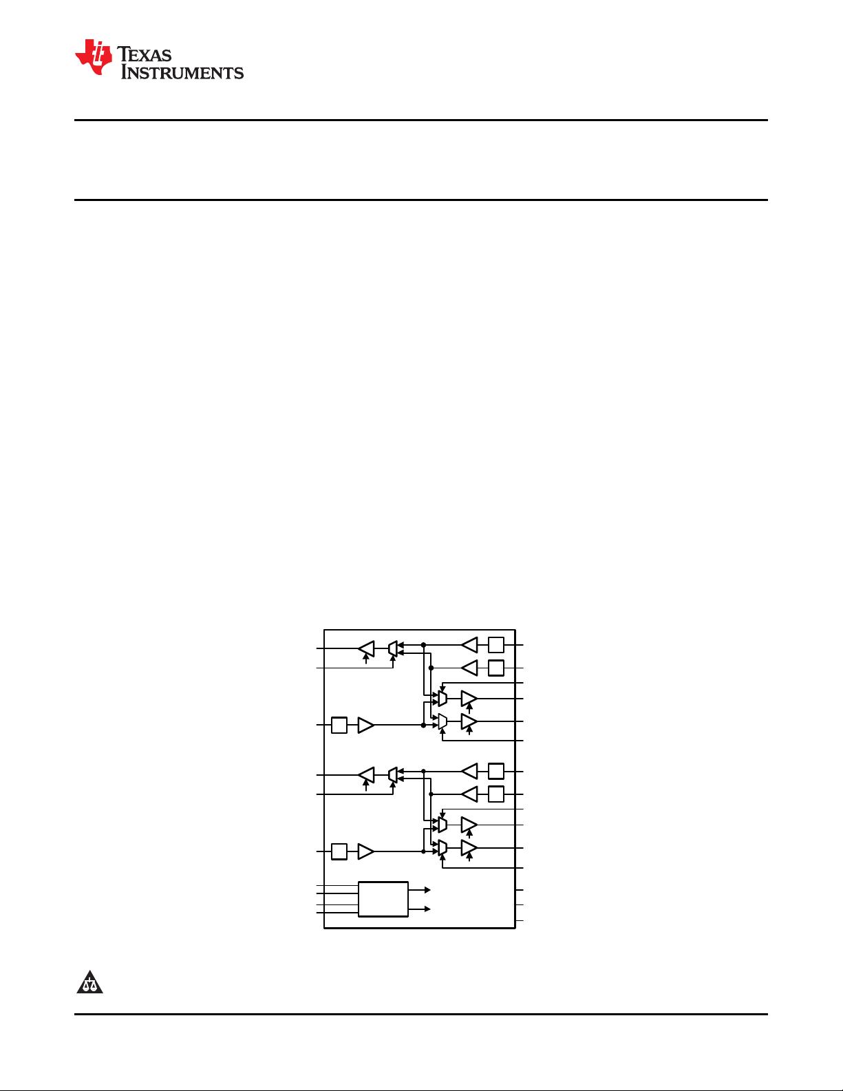
PRE_S
LO_0 ±
MUX_S0
SIA_0 ±
SIB_0 ±
LB0A
LB0B
SOA_0 ±
EQ
EQ
EQ
SOB_0 ±
LI_0 ±
PRE_S
PRE_L
PRE_S
LO_1 ±
MUX_S1
SIA_1 ±
SIB_1 ±
LB1A
LB1B
SOA_1 ±
EQ
EQ
EQ
SOB_1 ±
LI_1 ±
PRE_S
PRE_L
Pre-emphasis
Control
PreL_0
PreS_1
PreS_0
PreL_1
PRE_S
PRE_L
V
CC
GND
Port 0
Port 1
RSV
Switch Side
Line Side
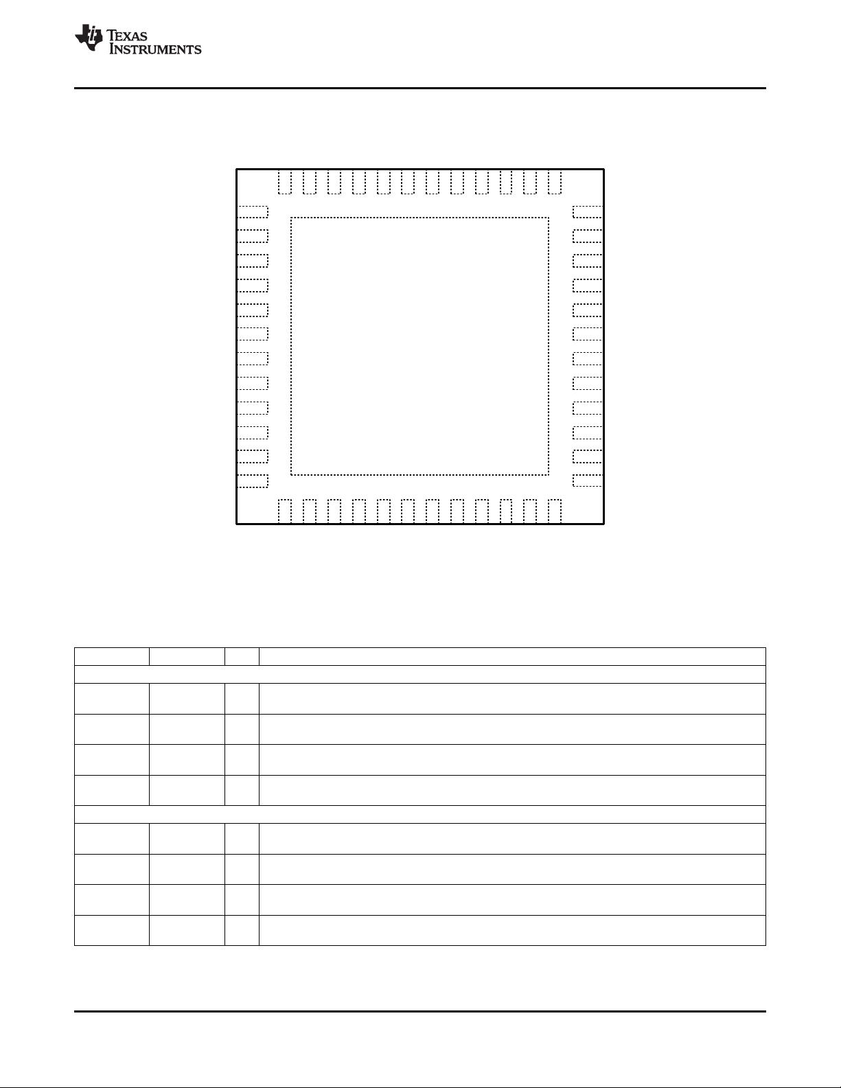
DS25MB200
www.ti.com
SNLS220G –MARCH 2006–REVISED APRIL 2013
DS25MB200 Dual 2.5 Gbps 2:1/1:2 CML Mux/Buffer with Transmit Pre-Emphasis and
Receive Equalization
Check for Samples: DS25MB200
1
FEATURES
DESCRIPTION
The DS25MB200 is a dual signal conditioning 2:1
2
• 0.6–2.5 Gbps Low Jitter Operation
multiplexer and 1:2 fan-out buffer designed for use in
• Fixed Input Equalization
backplane redundancy applications. Signal
• Programmable Output Pre-Emphasis
conditioning features include input equalization and
programmable output pre-emphasis that enable data
• Independent Switch and Line Side Pre-
communication in FR4 backplanes up to 2.5 Gbps.
Emphasis Controls
Each input stage has a fixed equalizer to reduce ISI
• Programmable Switch-Side Loopback Modes
distortion from board traces. All output drivers have 4
• On-Chip Terminations
selectable steps of pre-emphasis to compensate for
transmission losses from long FR4 backplanes and
• HBM ESD Rating 6 kV on All Pins
reduce deterministic jitter. The pre-emphasis levels
• +3.3V Supply
can be independently controlled for the line-side and
• Lead-Less WQFN-48 Package (7mm x 7mm x
switch-side drivers. The internal loopback paths from
0.8mm, 0.5mm Pitch)
switch-side input to switch-side output enable at-
speed system testing. All receiver inputs are internally
• -40°C to +85°C Operating Temperature Range
terminated with 100Ω differential terminating
resistors. All drivers are internally terminated with
APPLICATIONS
50Ω to V
CC
.
• Backplane or Cable Driver
• Redundancy and Signal Conditioning
Applications
Functional Block Diagram
All CML inputs and outputs must be AC coupled for optimal performance.
1
Please be aware that an important notice concerning availability, standard warranty, and use in critical applications of
Texas Instruments semiconductor products and disclaimers thereto appears at the end of this data sheet.
2All trademarks are the property of their respective owners.
PRODUCTION DATA information is current as of publication date.
Copyright © 2006–2013, Texas Instruments Incorporated
Products conform to specifications per the terms of the Texas
Instruments standard warranty. Production processing does not
necessarily include testing of all parameters.
剩余15页未读,继续阅读
资源评论

 qq_335607272023-02-15#完美解决问题 #运行顺畅 #内容详尽 #全网独家 #注释完整
- m0_745259962023-02-15#完美解决问题 #运行顺畅 #内容详尽 #注释完整
- CSDN_1872023-02-15#完美解决问题 #运行顺畅 #内容详尽 #全网独家 #注释完整
- 2301_763960562023-02-15#完美解决问题 #运行顺畅 #内容详尽 #全网独家 #注释完整

不觉明了
- 粉丝: 4780
- 资源: 5759


最新资源
- 基于Java和Kotlin的炉石传说自动化脚本项目源码+说明文档.zip
- 实习日报12.2.docx
- GO语言基础、学习笔记、项目规范.zip
- 免费功能一定要安装(安装上不用管)_sign.apk
- Goutte,一个简单的 PHP Web 爬虫.zip
- JAVA的Springboot个人博客系统源码带本地搭建教程数据库 MySQL源码类型 WebForm
- 2024-12-2 二阶问题(复杂区域)
- 架构师学习笔记,涵盖JAVA基础、MySQL、Spring、SpringBoot、SpringCloud、SpringCloudAlibaba、Redis、Kafka、设计模式、JVM等
- 开卡工具SM2258XT(AD)-B16A-PKGT1216A-FWT1125A0
- 电力场景变电站红外检测数据集VOC+YOLO格式6042张21类别.zip
资源上传下载、课程学习等过程中有任何疑问或建议,欢迎提出宝贵意见哦~我们会及时处理!
点击此处反馈


