TI-SN65MLVD129.pdf
需积分: 8 25 浏览量
2023-02-08
23:08:51
上传
评论 4
收藏 1.08MB PDF 举报


www.ti.com
FEATURES
APPLICATIONS
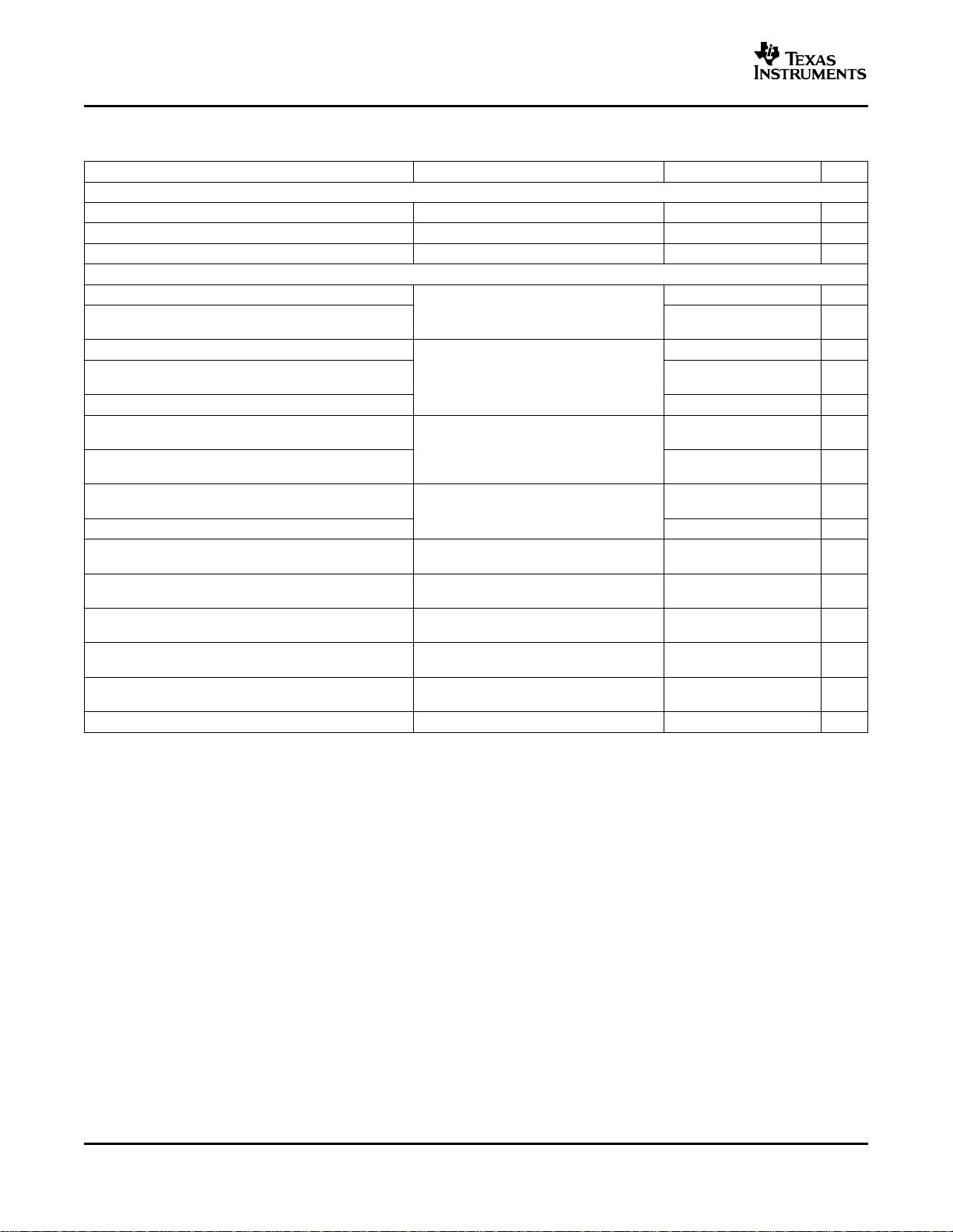
LOGIC DIAGRAM
EN1
EN2
EN3
EN4
EN5
EN6
EN7
EN8
1D
1A
1B
2A
2B
3A
3B
4A
4B
5A
5B
6A
6B
7A
7B
8A
8B
EN1
EN2
EN3
EN4
EN5
EN6
EN7
EN8
2 D
1A
1B
2A
2B
3A
3B
4A
4B
5A
5B
6A
6B
7A
7B
8A
8B
1 D
SN65MLVD128 SN65MLVD129
SN65MLVD128
SN65MLVD129
SLLS586 – MARCH 2004
1:8 LVTTL TO M-LVDS REPEATER DUAL 1:4 LVTTL TO M-LVDS REPEATER
• Bus Pins High Impedance When Disabled or
V
CC
≤ 1.5 V
• LVTTL Receiver and Eight Line Drivers
Configured as an 8-Port M-LVDS Repeater – • Independent Enables for each Driver
SN65MLVD128
• Output-to-Ouput Skew t
sk(o)
≤ 160 ps
• 2 LVTTL Receivers and Eight Line Drivers Part-to-Part Skew t
sk(pp)
≤ 800 ps
Configured as Dual 4-Port M-LVDS Repeaters
• Single 3.3-V Voltage Supply
– SN65MLVD129
• Bus Pin ESD Protection Exceeds 9 kV
• Drivers Meet or Exceed the M-LVDS Standard
• Packaged in 48-Pin TSSOP (DGG)
(TIA/EIA-899)
• Low-Voltage Differential 30- Ω to 55- Ω Line
Drivers for Data Rates
(1)
Up to 250 Mbps or
• AdvancedTCA™ ( ATCA™) Clock Bus Driver
Clock Frequencies Up to 125 MHz
• Clock Distribution
• Power Up/Down Glitch Free
• Data and Clock Repeating Over Backplanes
• Controlled Driver Output Voltage Transition
and Cables
Times for Improved Signal Quality
• Cellular Base Stations
(1) The data rate of a line, is the number of voltage transitions
• Central Office Switches
that are made per second expressed in the units bps (bits per
• Network Switches and Routers
second).
Please be aware that an important notice concerning availability, standard warranty, and use in critical applications of Texas
Instruments semiconductor products and disclaimers thereto appears at the end of this data sheet.
AdvancedTCA, ATCA are trademarks of PCI Industrial Computer Manufacturers Group.
PRODUCTION DATA information is current as of publication date.
Copyright © 2004, Texas Instruments Incorporated
Products conform to specifications per the terms of the Texas
Instruments standard warranty. Production processing does not
necessarily include testing of all parameters.
剩余21页未读,继续阅读
资源评论


