没有合适的资源?快使用搜索试试~ 我知道了~
TI-DRV401.pdf
需积分: 5 0 下载量 47 浏览量
2022-12-06
22:44:55
上传
评论 4
收藏 2.26MB PDF 举报
温馨提示
试读
37页
TI-DRV401.pdf
资源推荐
资源详情
资源评论
FEATURES
D DESIGNED FOR SENSORS FROM
VACUUMSCHMELZE (VAC)
D SINGLE SUPPLY: 5V
D POWER OUTPUT: H-Bridge
D DESIGNED FOR DRIVING INDUCTIVE LOADS
D EXCELLENT DC PRECISION
D WIDE SYSTEM BANDWIDTH
D HIGH-RESOLUTION, LOW-TEMPERATURE
DRIFT
D BUILT-IN DEGAUSS SYSTEM
D EXTENSIVE FAULT DETECTION
D EXTERNAL HIGH-POWER DRIVER OPTION
APPLICATIONS
D GENERATOR/ALTERNATOR MONITORING
AND CONTROL
D FREQUENCY AND VOLTAGE INVERTERS
D MOTOR DRIVE CONTROLLERS
D SYSTEM POWER CONSUMPTION
D PHOTOVOLTAIC SYSTEMS
DESCRIPTION
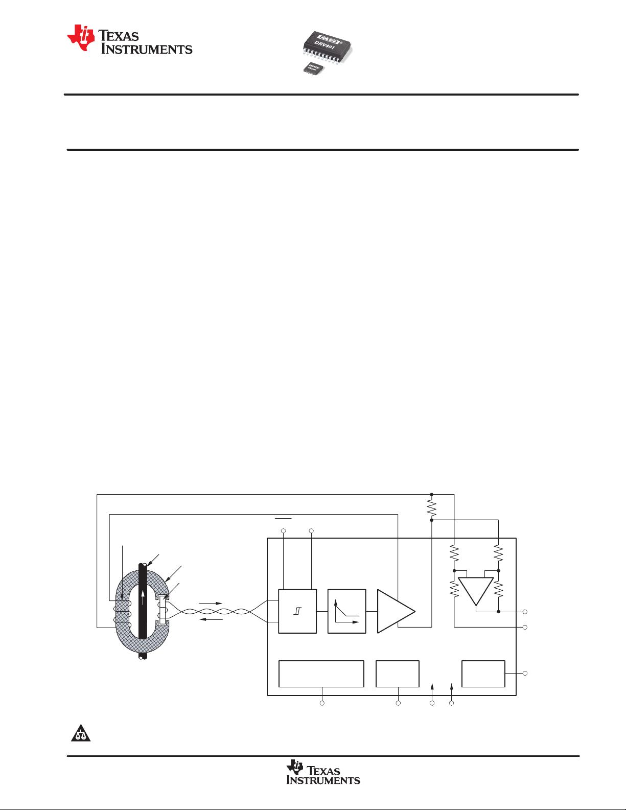
The DRV401 is designed to control and process signals
from specific magnetic current sensors made by
Vacuumschmelze GmbH & Co. KG (VAC). A variety of
current ranges and mechanical configurations are
available. Combined with a VAC sensor, the DRV401
monitors both ac and dc currents to high accuracy.
Provided functions include: probe excitation, signal
conditioning of the probe signal, signal loop amplifier, an
H-bridge driver for the compensation coil, and an analog
signal output stage that provides an output voltage
proportional to the primary current. It offers overload and
fault detection, as well as transient noise suppression.
The DRV401 can directly drive the compensation coil, or
connect to external power drivers. Therefore, the DRV401
combines with sensors to measure small to very large
currents.
To maintain the highest accuracy, the DRV401 can
demagnetize (degauss) the sensor at power-up and on
demand.
Integrator
Filter
Probe
Interface
H−Bridge
Driver
V
OUT
REF
IN
I
COMP2
R
S
I
COMP1
Compensation
Patents Pending.
Diff
Amp
Timing, Error Detection,
and Power Control
Degauss V
REF
V
REF
GND+5V
IS2
IS1
DRV401
I
P
Compensation Winding
Magnetic Core
Primary Winding
Field Probe
PWM PWM
DRV401
SBVS070B − JUNE 2006 − REVISED MAY 2009
Sensor Signal Conditioning IC for
Closed-Loop Magnetic Current Sensor
www.ti.com
Copyright 2006−2009, Texas Instruments Incorporated
Please be aware that an important notice concerning availability, standard warranty, and use in critical applications of Texas Instruments
semiconductor products and disclaimers thereto appears at the end of this data sheet.
PowerPAD is a trademark of Texas Instruments. All other trademarks are the property of their respective owners.
! !
"#$%
SBVS070B − JUNE 2006 − REVISED MAY 2009
www.ti.com
2
ABSOLUTE MAXIMUM RATINGS
(1)
Supply Voltage +7V. . . . . . . . . . . . . . . . . . . . . . . . . . . . . . . . . . . . . . .
Signal Input Terminals:
Voltage
(2)
−0.5V to V
DD
+ 0.5V. . . . . . . . . . . . . . . . . . . . . . . . . . .
Differential Amplifier
(3)
−10V to +10V. . . . . . . . . . . . . . . . . . . . . .
Current at IS1 and IS2 ±75mA. . . . . . . . . . . . . . . . . . . . . . . . . . . . .
Current (pins other than IS1 and IS2)
(2)
±25mA. . . . . . . . . . . . . .
I
COMP
Short Circuit
(4)
+250mA. . . . . . . . . . . . . . . . . . . . . . . . . . . . .
Operating Junction Temperature −50°C to +150°C. . . . . . . . . . . . .
Storage Temperature −55°C to +150°C. . . . . . . . . . . . . . . . . . . . . . .
ESD Rating:
Human Body Model (HBM)
Pins IA
IN1
and IA
IN2
Only 1kV. . . . . . . . . . . . . . . . . . . . . . . . . . .
All Other Pins 4kV. . . . . . . . . . . . . . . . . . . . . . . . . . . . . . . . . . . . .
(1)
Stresses above these ratings may cause permanent damage.
Exposure to absolute maximum conditions for extended periods
may degrade device reliability. These are stress ratings only, and
functional operation of the device at these or any other conditions
beyond those specified is not supported.
(2)
Input terminals are diode-clamped to the power-supply rails.
Input signals that can swing more than 0.5V beyond the supply
rails must be current limited, except for the differential amplifier
input pins.
(3)
These inputs are not internally protected against over voltage.
The differential amplifier input pins must be limited to 5mA, max or
±10V, max.
(4)
Power-limited; observe maximum junction temperature.
This integrated circuit can be damaged by ESD. Texas
Instruments recommends that all integrated circuits be
handled with appropriate precautions. Failure to observe
proper handling and installation procedures can cause damage.
ESD damage can range from subtle performance degradation to
complete device failure. Precision integrated circuits may be more
susceptible to damage because very small parametric changes could
cause the device not to meet its published specifications.
ORDERING INFORMATION
(1)
PRODUCT PACKAGE-LEAD
PACKAGE
DESIGNATOR
PACKAGE
MARKING
DRV401
QFN-20
(5mm x 5mm)
RGW HAAQ
DRV401 SO-20 DWP DRV401A
(1)
For the most current package and ordering information see the
Package Option Addendum at the end of this document, or see
the TI web site at www.ti.com.
"#$%
SBVS070B − JUNE 2006 − REVISED MAY 2009
www.ti.com
3
ELECTRICAL CHARACTERISTICS
Boldface limits apply over the specified temperature range: T
J
= −40°C to +125°C.
At T
A
= +25°C and V
DD1
= V
DD2
= +5V with external 100kHz filter BW, and zero output current I
COMP
, unless otherwise noted.
DRV401
PARAMETER CONDITIONS MIN TYP MAX
UNITS
DIFFERENTIAL AMPLIFIER R
L
= 10kΩ to 2.5V, V
REFIN
= 2.5V
OFFSET VOLTAGE
Offset Voltage, RTO
(1)(2)
V
OS
Gain 4V/V ±0.01 ±0.1 mV
Drift, RTO
(2)
dV
OS
/dT ±0.1 ±1
(3)
µV/°C
vs Common-Mode, RTO CMRR −1V to +6V, V
REF
= 2.5V ±50 ±250 µV/V
vs Power-Supply, RTO PSRR V
REF
not included ±4 ±50 µV/V
SIGNAL INPUT
Common-Mode Voltage Range −1 (V
DD
) + 1 V
SIGNAL OUTPUT
Signal Over-Range Indication (OVER-RANGE), Delay
(2)
V
IN
= 1V Step, See Notes 2 and 3 2.5 to 3.5 µs
Voltage Output Swing From Negative Rail
(2)
,
OVER-RANGE Trip Level
I = +2.5mA, CMP Trip Level +48 +85 mV
Voltage Output Swing From Positive Rail
(2)
,
OVER-RANGE Trip Level
I = −2.5mA, CMP Trip Level V
DD
− 85 V
DD
− 48 mV
Short-Circuit Current
(2)
I
SC
V
OUT
Connected To GND −18 mA
V
OUT
Connected To V
DD
+20 mA
Gain, V
OUT
/V
IN_DIFF
4 V/V
Gain Error ±0.02 ±0.3 %
Gain Error Drift ±0.1 ppm/°C
Linearity Error R
L
= 1kΩ 10 ppm
FREQUENCY RESPONSE
Bandwidth
(2)
BW
−3dB
2 MHz
Slew Rate
(2)
SR CMVR = −1V to = +4V 6.5 V/µs
Settling Time, Large-Signal
(2)
dV ± 2V to 1%, No External Filter 0.9 µs
Settling Time
(2)
dV ± 0.4V to 0.01% 14 µs
INPUT RESISTANCE
Differential 16.5 20 23.5 kΩ
Common-Mode 41 50 59 kΩ
External Reference Input 41 50 59 kΩ
NOISE
Output Voltage Noise Density, f = 1kHz, RTO
(2)
e
n
Compensation Loop Disabled 170 nV/√Hz
COMPENSATION LOOP
DC STABILITY Probe f = 250kHz, R
LOAD
= 20Ω
Offset Error
(4)
Deviation from 50% PWM, Pin Gain = L 0.03 %
Offset Error Drift
(2)
Deviation from 50% PWM, Pin Gain = L 7.5 ppm/°C
Gain, Pin Gain = L
(2)
|V
ICOMP1
| − |V
ICOMP2
| −200 25 200 ppm/V
Power-Supply Rejection Ratio
PSRR
Probe Loop f = 250kHz
500 ppm/V
FREQUENCY RESPONSE
Open-Loop Gain, Two Modes, 7.8kHz Pin Gain H/L
24/32 dB
PROBE COIL LOOP
Input Voltage Clamp Range Field Probe Current < 50mA −0.7 to V
DD
+ 0.7 V
Internal Resistor, IS1 or IS2 to V
DD1
(2)
R
HIGH
47 59 71 Ω
Internal Resistor, IS1 or IS2 to GND1
(2)
R
LOW
60 75 90 Ω
Resistance Mismatch Between IS1 and IS2
(2)
ppm of R
HIGH
+ R
LOW
300 1500 ppm
Total Input Resistance
(3)
134 200 W
Comparator Threshold Current
(3)
22 28 34 mA
Minimum Probe Loop Half-Cycle
(2)
250 280 310 ns
Probe Loop Minimum Frequency 250 kHz
No Oscillation Detect (Error) Suppression 35 µs
COMPENSATION COIL DRIVER, H-BRIDGE
Peak Current
(2)
V
ICOMP1
− V
ICOMP2
= 4.0V
PP
250 mA
Voltage Swing 20Ω Load 4.2 V
PP
Output Common-Mode Voltage V
DD2
/2 V
Wire Break Detect, Threshold Current
(5)
I
COMP1
and I
COMP2
Railed 33 57 mA
"#$%
SBVS070B − JUNE 2006 − REVISED MAY 2009
www.ti.com
4
ELECTRICAL CHARACTERISTICS (continued)
Boldface limits apply over the specified temperature range, T
J
= −40°C to +125°C, with zero output current I
COMP
.
At T
A
= +25°C and V
DD1
= V
DD2
= +5V with external 100kHz filter BW, unless otherwise noted.
DRV401
PARAMETER CONDITIONS MIN TYP MAX
UNITS
VOLTAGE REFERENCE
Voltage
(2)
No Load 2.495 2.5 2.505 V
Drift
(2)
No Load ±5 ±50 ppm/°C
PSRR
(2)
±15 ±200 µV/V
Load Regulation
(2)
Load to GND/V
DD
, dI = 0mA to 5mA 0.15 mV/mA
Short-Circuit Current I
SC
REF
OUT
Connected to V
DD
+20 mA
REF
OUT
Connected to GND −18 mA
DEMAGNETIZATION
Duration See Timing Diagram 106 130
(3)
ms
DIGITAL I/O
LOGIC INPUTS (DEMAG, GAIN, and CCdiag Pins) CMOS Type Levels
Pull-Up High Current (CCdiag) 3.5 < V
IN
< V
DD
160 µA
Pull-Up Low Current (CCdiag) 0 < V
IN
< 1.5 5 µA
Logic Input Leakage Current 0 < V
IN
< V
DD
0.01 5 µA
Logic Level, Input: L/H 2.1/2.8 V
Hysteresis 0.7 V
OUTPUTS (ERROR AND OVER-RANGE Pins)
Logic Level, Output: L 4mA Sink 0.3 V
Logic Level, Output: H No Internal Pull-Up
OUTPUTS (PWM and PWM Pins) Push-Pull Type
Logic Level L 4mA Sink 0.2 V
Logic Level H 4mA Source (V
DD
) − 0.4 V
POWER SUPPLY
Specified Voltage Range V
DD
4.5 5 5.5 V
Power-On Reset Threshold V
RST
1.8 V
Quiescent Current [I(V
DD1
) + I(V
DD2
)] I
Q
I
COMP
= 0mA, Sensor Not Connected 6.8 mA
Brownout Voltage Level
(2)
4 V
Brownout Indication Delay 135 µs
TEMPERATURE RANGE
Specified Range
T
J
−40 +125 °C
Operating Range
T
J
−50 +150 °C
Package Thermal Resistance
QFN Surface-Mount
q
JA
See Note 6 40 °C/W
SO PowerPAD Surface-Mount
q
JA
See Note 6 27 °C/W
(1)
Parameter value referred to output (RTO).
(2)
See Typical Characteristic curves.
(3)
Total input resistance and comparator threshold current are inversely related. See Figure 2a.
(4)
For VAC sensors, 0.2% of PWM offset approximately corresponds to 10mA primary current offset per winding.
(5)
See Compensation Driver section in Applications Information.
(6)
See Applications Information section for information on power dissipation, layout considerations, and proper PCB soldering and heat-sinking technique.
"#$%
SBVS070B − JUNE 2006 − REVISED MAY 2009
www.ti.com
5
PIN CONFIGURATIONS
Top View RGW Top View DWP
ERROR
DEMAG
GAIN
REF
OUT
REF
IN
V
DD1
OVER−RANGE
CCdiag
V
DD2
I
COMP1
Exposed
Thermal Pad
on Underside,
Connect
to GND1
PWM
PWM
IS1
GND1
IS2
V
OUT
IA
IN2
IA
IN1
GND2
I
COMP2
6
7
8
9
10
1
2
3
4
5
15
14
13
12
11
20
19
18
17
16
QFN−20 (5mm x 5mm)
PWM
PWM
ERROR
DEMAG
GAIN
REF
OUT
REF
IN
V
OUT
IA
IN2
IA
IN1
IS1
GND1
IS2
V
DD1
OVER−RANGE
CCdiag
V
DD2
I
COMP1
I
COMP2
GND2
1
2
3
4
5
6
7
8
9
10
20
19
18
17
16
15
14
13
12
11
Wide−Body SO−20
Exposed
Thermal Pad
on Underside,
Connect
to GND1
PIN ASSIGNMENTS
NAME RGW DWP DESCRIPTION
ERROR 1 3 Error flag: open-drain output, see the Error Conditions section.
DEMAG 2 4 Control input, see the Demagnetization section.
GAIN 3 5 Control input for open-loop gain: low = normal, high = −8dB.
REF
OUT
4 6 Output for internal 2.5V reference voltage.
REF
IN
5 7 Input for zero reference to differential amplifier.
V
OUT
6 8 Output for differential amplifier.
IA
IN2
7 9 Noninverting input of differential amplifier.
IA
IN1
8 10 Inverting input of differential amplifier.
GND2 9 11 Ground connection. Connect to GND1.
I
COMP2
10 12 Output 2 of compensation coil driver.
I
COMP1
11 13 Output 1 of compensation coil driver.
V
DD2
12 14 Supply voltage. Connect to V
DD1
.
CCdiag 13 15 Control input for wire-break detection: high = enable.
OVER−RANGE 14 16 Open-drain output for over-range indication: low = over-range.
V
DD1
15 17 Supply voltage.
IS2 16 18 Probe connection 2.
GND1 17 19 Ground connection.
IS1 18 20 Probe connection 1.
PWM 19 1 PWM output from probe circuit (inverted).
PWM 20 2 PWM output from probe circuit.
Exposed Thermal Pad — — Connect to GND1.
剩余36页未读,继续阅读
资源评论
不觉明了
- 粉丝: 3188
- 资源: 5486
上传资源 快速赚钱
- 我的内容管理 展开
- 我的资源 快来上传第一个资源
- 我的收益 登录查看自己的收益
- 我的积分 登录查看自己的积分
- 我的C币 登录后查看C币余额
- 我的收藏
- 我的下载
- 下载帮助
安全验证
文档复制为VIP权益,开通VIP直接复制
信息提交成功