TI-SN74LVC32373A.pdf
需积分: 5 157 浏览量
2022-11-28
13:04:05
上传
评论 4
收藏 784KB PDF 举报

www.ti.com
FEATURES
DESCRIPTION/ORDERING INFORMATION
SN74LVC32373A
32-BIT TRANSPARENT D-TYPE LATCH
WITH 3-STATE OUTPUTS
SCES575 – JUNE 2004 – REVISED AUGUST 2005
• Member of the Texas Instruments Widebus+™ • I
off
Supports Partial-Power-Down Mode
Family Operation
• Operates From 1.65 V to 3.6 V • Supports Mixed-Mode Signal Operation (5-V
Input and Output Voltages With 3.3-V V
CC
)
• Inputs Accept Voltages to 5.5 V
• Latch-Up Performance Exceeds 100 mA Per
• Max t
pd
of 4.2 ns at 3.3 V
JESD 78, Class II
• Typical V
OLP
(Output Ground Bounce) <0.8 V
• ESD Protection Exceeds JESD 22
at V
CC
= 3.3 V, T
A
= 25 ° C
– 2000-V Human-Body Model (A114-A)
• Typical V
OHV
(Output V
OH
Undershoot) >2 V at
V
CC
= 3.3 V, T
A
= 25 ° C – 1000-V Charged-Device Model (C101)
This 32-bit transparent D-type latch is designed for 1.65-V to 3.6-V V
CC
operation.
The SN74LVC32373A is particularly suitable for implementing buffer registers, I/O ports, bidirectional bus drivers,
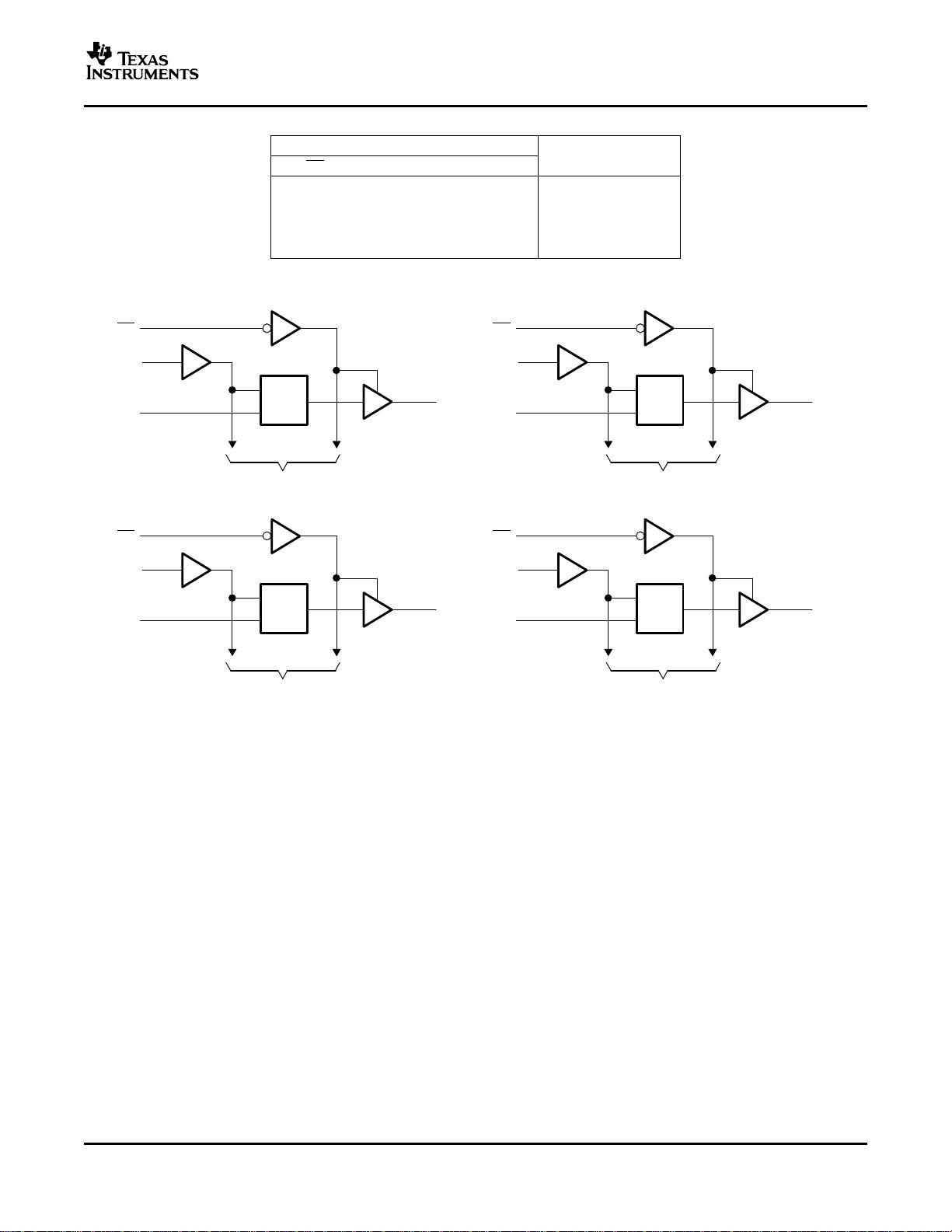
and working registers. It can be used as four 8-bit latches, two 16-bit latches, or one 32-bit latch. When the
latch-enable (LE) input is high, the Q outputs follow the data (D) inputs. When LE is taken low, the Q outputs are
latched at the levels set up at the D inputs.
A buffered output-enable ( OE) input can be used to place the eight outputs in either a normal logic state (high or
low logic levels) or the high-impedance state. In the high-impedance state, the outputs neither load nor drive the
bus lines significantly. The high-impedance state and increased drive provide the capability to drive bus lines
without interface or pullup components.
OE does not affect internal operations of the latch. Old data can be retained or new data can be entered while
the outputs are in the high-impedance state.
Inputs can be driven from either 3.3-V or 5-V devices. This feature allows the use of these devices as translators
in a mixed 3.3-V/5-V system environment.
This device is fully specified for partial-power-down applications using I
off
. The I
off
circuitry disables the outputs,
preventing damaging current backflow through the device when it is powered down.
To ensure the high-impedance state during power up or power down, OE should be tied to V
CC
through a pullup
resistor; the minimum value of the resistor is determined by the current-sinking capability of the driver.
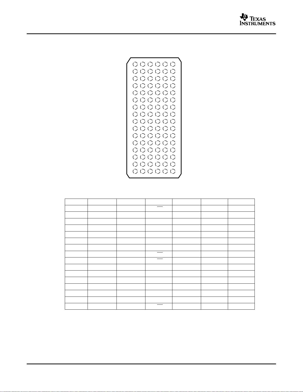
ORDERING INFORMATION
T
A
PACKAGE
(1)
ORDERABLE PART NUMBER TOP-SIDE MARKING
LFBGA – GKE SN74LVC32373AGKER
–40 ° C to 85 ° C Tape and reel NC373A
LFBGA – ZKE (Pb-free) SN74LVC32373AZKER
(1) Package drawings, standard packing quantities, thermal data, symbolization, and PCB design guidelines are available at
www.ti.com/sc/package.
Please be aware that an important notice concerning availability, standard warranty, and use in critical applications of Texas
Instruments semiconductor products and disclaimers thereto appears at the end of this data sheet.
Widebus+ is a trademark of Texas Instruments.
PRODUCTION DATA information is current as of publication date.
Copyright © 2004–2005, Texas Instruments Incorporated
Products conform to specifications per the terms of the Texas
Instruments standard warranty. Production processing does not
necessarily include testing of all parameters.
剩余12页未读,继续阅读


评论0
最新资源