TI-BQ26100.pdf
需积分: 10 117 浏览量
2022-10-31
21:52:08
上传
评论 5
收藏 996KB PDF 举报

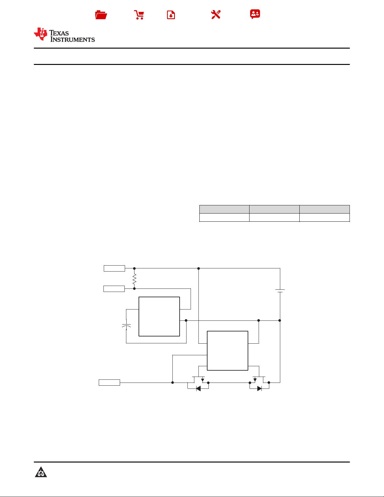
SDQ
P–
C1
0.1 Fm
+
VSS
CO
BAT
OC
DO
bq26100
SDQ
VSS
VSS
PWR
VSS
VSS
R1
4.7kW
P+
Protector
Product
Folder
Order
Now
Technical
Documents
Tools &
Software
Support &
Community
An IMPORTANT NOTICE at the end of this data sheet addresses availability, warranty, changes, use in safety-critical applications,
intellectual property matters and other important disclaimers. PRODUCTION DATA.
bq26100
SLUS696C –JUNE 2006–REVISED FEBRUARY 2019
bq26100 SHA-1/HMAC-based security and authentication IC with an SDQ interface
1
1 Features
1
• Provides authentication of battery packs through
SHA-1 engine based HMAC
• 160-byte one-time programmable (OTP), 16-bytes
EEPROM
• Internal time-base eliminates external crystal
oscillator
• Low-power operating modes:
– Active: < 50 μA
– Sleep: 8 μA typical
• Single-wire SDQ interface
• Powers directly from the communication bus
• 6-lead VSON package
2 Applications
• Cellular phones
• PDA and smart phones
• MP3 players
• Digital cameras
• Internet appliances
• Handheld devices
3 Description
The bq26100 device provides a method to
authenticate battery packs, ensuring that only packs
manufactured by authorized sub-contractors are used
in the end application. The security is achieved using
the SHA-1 hash function inside the widely adopted
keyed-hash message authentication code (HMAC)
construction. A unique 128-bit key is stored in each
bq26100 device, allowing the host to authenticate
each pack.
The bq26100 device communicates to the system
over a simple one-wire bi-directional serial interface.
The 5-kbits/s SDQ bus interface reduces
communications overhead in the external
microcontroller. The bq26100 device also derives
power over the SDQ bus line via an external
capacitor.
Device Information
(1)
PART NUMBER PACKAGE BODY SIZE (NOM)
bq26100 VSON (6) 3.00 mm × 3.00 mm
(1) For all available packages, see the orderable addendum at
the end of the data sheet.
Simplified Schematic


剩余29页未读,继续阅读
资源评论


