没有合适的资源?快使用搜索试试~ 我知道了~
TI-LM2588.pdf
需积分: 8 0 下载量 170 浏览量
2022-10-23
13:45:01
上传
评论 5
收藏 2.26MB PDF 举报
温馨提示
试读
39页
TI-LM2588.pdf
资源详情
资源评论
Product
Folder
Order
Now
Technical
Documents
Tools &
Software
Support &
Community
本文档旨在为方便起见,提供有关 TI 产品中文版本的信息,以确认产品的概要。 有关适用的官方英文版本的最新信息,请访问 www.ti.com,其内容始终优先。 TI 不保证翻译的准确
性和有效性。 在实际设计之前,请务必参考最新版本的英文版本。
English Data Sheet: SNVS117
LM2588
ZHCS518E –APRIL 1998–REVISED JUNE 2019
具具有有关关断断功功能能的的 LM2588 5A 反反激激式式稳稳压压器器
1
1 特特性性
1
• 无需外部组件
• 标准电感器和变压器系列
• NPN 输出开关电流为 5A,可切断 65V 电压
• 宽输入电压范围:4V 至 40V
• 可调开关频率:100kHz 至 200kHz
• 外部关断功能
• 关断时消耗电流小于 60μA
• 频率同步
• 可改进瞬态响应、线路调节和电流限制的电流模式
操作
• 内部软启动功能可降低启动过程中的浪涌电流
• 通过电流限制、欠压锁定和热关断为输出晶体管提
供保护
• 在跨线路和负载条件下的最高系统输出电压容差为
±4%
• 使用 LM2588 并借助 WEBENCH
®
电源设计器创建
定制设计方案
2 典典型型 应应用用
• 反激式稳压器
• 正向转换器
• 多输出稳压器
• 简单升压稳压器
3 说说明明
LM2588 系列稳压器是专为反激式、升压和正向转换器
应用而设计的单片集成电路。该器件提供 4 种不同的
输出电压版本:3.3V、5V、12V 和可调节电压。
这些稳压器需要的外部组件很少,因此具有成本效益,
并且易于使用。此数据表中包含了典型的升压和反激式
稳压器电路。另外还列出了二极管和电容器以及标准电
感器和反激式变压器系列的选择指南,这些器件专用于
与上述开关稳压器协同工作。
该电源开关是一款 5A NPN 器件,可切断 65V 电压。
电源开关由电流和热限制电路以及欠压锁定电路进行保
护。此 IC 包含可调频率振荡器,其频率可编程为高达
200kHz。该振荡器还可与其他器件同步,从而可以在
同一开关频率下运行多个器件。
其他 功能 包括在启动期间降低浪涌电流的软启动模
式、用于改进抑制输入电压和输出负载瞬态的电流模式
控制功能,以及逐周期电流限制。该器件还具有关断引
脚,因此可以从外部关闭。在额定输入电压和输出负载
条件下,电源系统可确保 ±4% 的输出电压容差。
器器件件信信息息
(1)
器器件件型型号号 封封装装 封封装装尺尺寸寸((标标称称值值))
LM2588
TO-220 (7) 10.1mm × 8.89mm
DDPAK/TO-263 (7) 14.986mm × 10.16mm
(1) 如需了解所有可用封装,请参阅数据表末尾的可订购产品附
录。
反反激激式式稳稳压压器器
2
LM2588
ZHCS518E –APRIL 1998–REVISED JUNE 2019
www.ti.com.cn
Copyright © 1998–2019, Texas Instruments Incorporated
目目录录
1 特特性性.......................................................................... 1
2 典典型型 应应用用.................................................................. 1
3 说说明明.......................................................................... 1
4 修修订订历历史史记记录录 ........................................................... 2
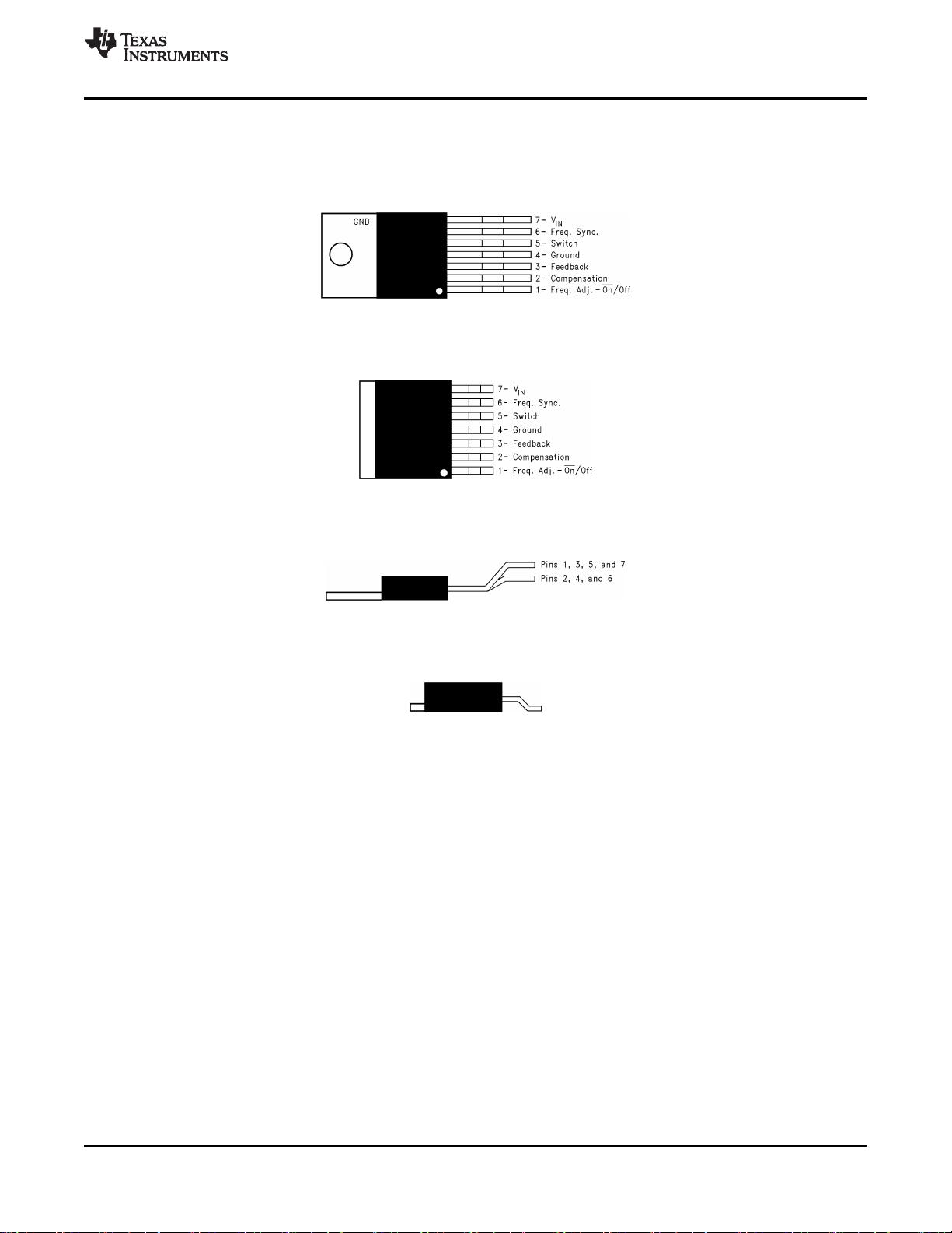
5 Pin Configurations................................................. 3
6 Specifications......................................................... 4
6.1 Absolute Maximum Ratings ...................................... 4
6.2 ESD Ratings.............................................................. 4
6.3 Recommended Operating Ratings............................ 4
6.4 Electrical Characteristics: 3.3 V ................................ 5
6.5 Electrical Characteristics: 5 V ................................... 5
6.6 Electrical Characteristics: 12 V ................................. 6
6.7 Electrical Characteristics: Adjustable........................ 6
6.8 Electrical Characteristics: All Output Voltage Versions
...................................................................................7
6.9 Typical Characteristics.............................................. 9
7 Detailed Description ............................................ 12
7.1 Overview ................................................................. 12
7.2 Functional Block Diagram ....................................... 12
7.3 Feature Description................................................. 12
8 Application and Implementation ........................ 18
8.1 Application Information............................................ 18
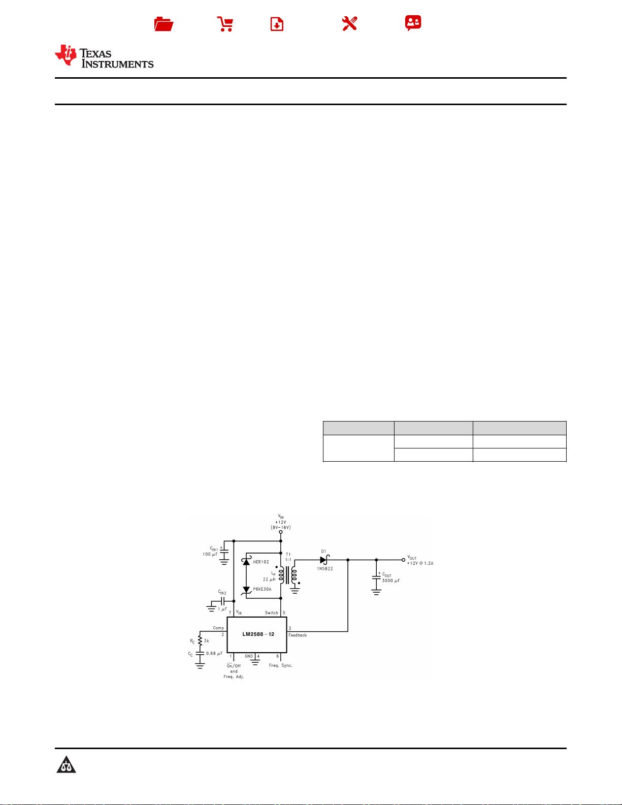
8.2 Typical Applications ............................................... 18
8.3 System Examples ................................................... 28
9 Layout ................................................................... 29
9.1 Layout Guidelines ................................................... 29
9.2 Layout Example ...................................................... 29
9.3 Heat Sink/Thermal Considerations ......................... 29
10 器器件件和和文文档档支支持持 ..................................................... 31
10.1 器件支持................................................................ 31
10.2 接收文档更新通知 ................................................. 31
10.3 社区资源................................................................ 31
10.4 商标 ....................................................................... 31
10.5 静电放电警告......................................................... 32
10.6 Glossary................................................................ 32
11 机机械械、、封封装装和和可可订订购购信信息息....................................... 32
4 修修订订历历史史记记录录
注:之前版本的页码可能与当前版本有所不同。
Changes from Revision D (April 2013) to Revision E Page
• 仅有编辑更改;无技术性修订 ................................................................................................................................................. 1
• 已添加 添加了 WEBENCH 链接 ............................................................................................................................................. 1
Changes from Revision C (April 2013) to Revision D Page
• 将美国国家半导体数据表的布局更改为 TI 格式 ...................................................................................................................... 1
3
LM2588
www.ti.com.cn
ZHCS518E –APRIL 1998–REVISED JUNE 2019
Copyright © 1998–2019, Texas Instruments Incorporated
5 Pin Configurations
NDZ Package
7-Pin TO-220
Top View, Bent, Staggered Leads
KTW Package
7-Pin DDPAK/TO-263
Top View
NDZ Package
7-Pin TO-220
Side View; Bent, Staggered Leads
KTW Package
7-Pin DDPAK/TO-263
Side View
4
LM2588
ZHCS518E –APRIL 1998–REVISED JUNE 2019
www.ti.com.cn
Copyright © 1998–2019, Texas Instruments Incorporated
(1) Absolute Maximum Ratings indicate limits beyond which damage to the device may occur. These ratings apply when the current is
limited to less than 1.2 mA for pins 1, 2, 3, and 6. Operating ratings indicate conditions for which the device is intended to be functional,
but device parameter specifications may not be ensured under these conditions. For ensured specifications and test conditions, see the
Electrical Characteristics.
(2) If Military/Aerospace specified devices are required, contact the TI Sales Office/ Distributors for availability and specifications.
(3) Note that switch current and output current are not identical in a step-up regulator. Output current cannot be internally limited when the
LM2588 is used as a step-up regulator. To prevent damage to the switch, the output current must be externally limited to 5A. However,
output current is internally limited when the LM2588 is used as a flyback regulator (see the section for more information).
(4) The junction temperature of the device (T
J
) is a function of the ambient temperature (T
A
), the junction-to-ambient thermal resistance
(θ
JA
), and the power dissipation of the device (P
D
). A thermal shutdown will occur if the temperature exceeds the maximum junction
temperature of the device: P
D
× θ
JA
+ T
A(MAX)
≥ T
J(MAX)
. For a safe thermal design, check that the maximum power dissipated by the
device is less than: P
D
≤ [T
J(MAX)
− T
A(MAX)
]/θ
JA
. When calculating the maximum allowable power dissipation, derate the maximum
junction temperature—this ensures a margin of safety in the thermal design.
6 Specifications
6.1 Absolute Maximum Ratings
See
(1)(2)
Input Voltage −0.4V ≤ V
IN
≤ 45V
Switch Voltage −0.4V ≤ V
SW
≤ 65V
Switch Current
(3)
Internally Limited
Compensation Pin Voltage −0.4V ≤ V
COMP
≤ 2.4V
Feedback Pin Voltage −0.4V ≤ V
FB
≤ 2 V
OUT
ON /OFF Pin Voltage −0.4V ≤ V
SH
≤ 6V
Sync Pin Voltage −0.4V ≤ V
SYNC
≤ 2V
Power Dissipation
(4)
Internally Limited
Storage Temperature Range −65°C to +150°C
Lead Temperature (Soldering, 10 sec.) 260°C
Maximum Junction Temperature
(4)
150°C
(1) JEDEC document JEP155 states that 500-V HBM allows safe manufacturing with a standard ESD control process.
6.2 ESD Ratings
VALUE UNIT
V
(ESD)
Electrostatic discharge
(minimum)
Human-body model (HBM), per ANSI/ESDA/JEDEC JS-001
(1)
(C = 100 pF, R = 1.5 kΩ)
2000 V
6.3 Recommended Operating Ratings
Supply Voltage 4V ≤ V
IN
≤ 40V
Output Switch Voltage 0V ≤ V
SW
≤ 60V
Output Switch Current I
SW
≤ 5.0A
Junction Temperature Range −40°C ≤ T
J
≤ +125°C
5
LM2588
www.ti.com.cn
ZHCS518E –APRIL 1998–REVISED JUNE 2019
Copyright © 1998–2019, Texas Instruments Incorporated
(1) External components such as the diode, inductor, input and output capacitors can affect switching regulator performance. When the
LM2588 is used as shown in Figure 54 and Figure 55, system performance will be as specified by the system parameters.
(2) All room temperature limits are 100% production tested, and all limits at temperature extremes are specified via correlation using
standard Statistical Quality Control (SQC) methods.
(3) A 1.0 MΩ resistor is connected to the compensation pin (which is the error amplifier output) to ensure accuracy in measuring A
VOL
.
6.4 Electrical Characteristics: 3.3 V
Specifications with standard type face are for T
J
= 25°C, and those in boldtype face apply over full Operating Temperature
Range. Unless otherwise specified, V
IN
= 5V.
PARAMETER TEST CONDITIONS TYP MIN MAX UNIT
SYSTEM PARAMETERS Test Circuit of Figure 54
(1)
V
OUT
Output Voltage V
IN
= 4V to 12V
I
LOAD
= 400 mA to 1.75A
3.3 3.17/3.14 3.43/3.46 V
ΔV
OUT
/
ΔV
IN
Line Regulation V
IN
= 4V to 12V
I
LOAD
= 400 mA
20 50/100 mV
ΔV
OUT
/
ΔI
LOAD
Load Regulation V
IN
= 12V
I
LOAD
= 400 mA to 1.75A
20 50/100 mV
η Efficiency V
IN
= 12V, I
LOAD
= 1A 75 %
UNIQUE DEVICE PARAMETERS
(2)
V
REF
Output Reference
Voltage
Measured at Feedback Pin
V
COMP
= 1.0V
3.3 3.242/3.234 3.358/3.366 V
ΔV
REF
Reference Voltage Line
Regulation
V
IN
= 4V to 40V
2.0 mV
G
M
Error Amp
Transconductance
I
COMP
= −30 μA to +30 μA
V
COMP
= 1.0V
1.193 0.678 2.259 mmho
A
VOL
Error Amp Voltage
Gain
V
COMP
= 0.5V to 1.6V
R
COMP
= 1.0 MΩ
(3)
260 151/75 V/V
(1) External components such as the diode, inductor, input and output capacitors can affect switching regulator performance. When the
LM2588 is used as shown in Figure 54 and Figure 55, system performance will be as specified by the system parameters.
(2) All room temperature limits are 100% production tested, and all limits at temperature extremes are specified via correlation using
standard Statistical Quality Control (SQC) methods.
(3) A 1.0 MΩ resistor is connected to the compensation pin (which is the error amplifier output) to ensure accuracy in measuring A
VOL
.
6.5 Electrical Characteristics: 5 V
Specifications with standard type face are for T
J
= 25°C, and those in bold type face apply over full Operating Temperature
Range. Unless otherwise specified, V
IN
= 5V.
PARAMETER TEST CONDITIONS TYP MIN MAX UNIT
SYSTEM PARAMETERS Test Circuit of Figure 54
(1)
V
OUT
Output Voltage V
IN
= 4V to 12V
I
LOAD
= 500 mA to 1.45A
5.0 4.80/4.75 5.20/5.25 V
ΔV
OUT
/
ΔV
IN
Line Regulation V
IN
= 4V to 12V
I
LOAD
= 500 mA
20 50/100 mV
ΔV
OUT
/
ΔI
LOAD
Load Regulation V
IN
= 12V
I
LOAD
= 500 mA to 1.45A
20 50/100 mV
η Efficiency V
IN
= 12V, I
LOAD
= 750 mA 80 %
UNIQUE DEVICE PARAMETERS
(2)
V
REF
Output Reference
Voltage
Measured at Feedback Pin
V
COMP
= 1.0V
5.0 4.913/4.900 5.088/5.100 V
ΔV
REF
Reference Voltage Line
Regulation
V
IN
= 4V to 40V
3.3 mV
G
M
Error Amp
Transconductance
I
COMP
= −30 μA to +30 μA
V
COMP
= 1.0V
0.750 0.447 1.491 mmho
A
VOL
Error Amp Voltage
Gain
V
COMP
= 0.5V to 1.6V
R
COMP
= 1.0 MΩ
(3)
165 99/49 V/V
剩余38页未读,继续阅读
安全验证
文档复制为VIP权益,开通VIP直接复制
信息提交成功
评论0
最新资源