


TPS63020
L1 L2
VIN VOUT
GND
V
IN
1.8 V to 5.5 V
V
OUT
3.3 V
L1
1.5 µH
C1
2×10 µF
C2
3×22 µF
VINA
C3
100 nF
EN
PS/SYNC
PGND
FB
PG
R1
1 0Ÿ
R2
180 NŸ
R3
1 0Ÿ
Power
Good
Output Current (A)
Efficiency (%)
0
10
20
30
40
50
60
70
80
90
100
100P 1m 10m 100m 1
Power-save mode enabled
D001
V
IN
= 1.8 V, V
OUT
= 2.5 V
V
IN
= 3.6 V, V
OUT
= 2.5 V
V
IN
= 2.4 V, V
OUT
= 4.5 V
V
IN
= 3.6 V, V
OUT
= 4.5 V
Product
Folder
Order
Now
Technical
Documents
Tools &
Software
Support &
Community
本文档旨在为方便起见,提供有关 TI 产品中文版本的信息,以确认产品的概要。 有关适用的官方英文版本的最新信息,请访问 www.ti.com,其内容始终优先。 TI 不保证翻译的准确
性和有效性。 在实际设计之前,请务必参考最新版本的英文版本。
English Data Sheet: SLVS916
TPS63020
,
TPS63021
ZHCSJG8I –JULY 2010–REVISED OCTOBER 2019
具具有有 4A 开开关关的的 TPS6302x 高高效效率率单单电电感感器器降降压压/升升压压转转换换器器
1
1 特特性性
1
• 输入电压范围:1.8V 至 5.5V
• 可调节输出电压:1.2V 至 5.5V
• V
IN
> 2.5V、V
OUT
= 3.3V 时,输出电流为 2A
• 在整个负载范围内具有高效率
– 静态工作电流:25μA
– 支持模式选择的省电模式
• 平均电流模式降压/升压架构
– 模式间自动转换
– 2.4MHz 固定频率工作
– 可同步
• 电源正常状态输出
• 安全、可靠运行 特性
– 过热和过压保护
– 关断期间负载断开
• 借助以下工具创建定制设计方案:
– TPS63020,使用 WEBENCH 电源设计器
– TPS63021,使用 WEBENCH 电源设计器
2 应应用用
• 电池供电设备前置稳压器:EPOS(便携式数据终
端、条形码扫描仪)、电子烟、单板计算机、IP 网
络摄像头、可视门铃、陆地移动无线电
• 稳压器:有线通信、无线通信、PLC、光学模块
• 超级电容器备用电源:电表、企业级固态硬盘
(SSD)
SPACE
3 说说明明
TPS6302x 器件可以为由两节或三节碱性电池、镍镉电
池或镍氢电池或单节锂离子电池或锂聚合物电池、超级
电容器或其他电源轨供电的产品提供电源解决方案。支
持高达 3A 的输出电流。使用电池时,可以放电到 2V
以下。该降压/升压转换器基于一个使用同步整流的固
定频率、脉宽调制 (PWM) 控制器来获得最高效率。在
负载电流较低的情况下,该转换器会进入节能模式,以
在宽负载电流范围内保持高效率。禁用省电模式则会强
制转换器以固定开关频率运行。开关的最大平均电流为
4A(典型值)。输出电压可通过外部电阻分频器进行
编程,或者在内部芯片上固定。转换器可被禁用以最大
限度地减少电池消耗。在关断期间,负载从电池上断
开。
TPS6302x 器件在自然通风环境下运行的温度范围为
–40°C 至 85°C。该器件采用 3mm × 4mm (DSJ) 14
引脚 VSON 封装。
器器件件信信息息
(1)
器器件件型型号号 输输出出电电压压 封封装装
TPS63020 可调节
VSON (14)
TPS63021 3.3V
(1) 要了解所有可用封装,请参见数据表末尾的可订购数据表。
空白
简简化化电电路路原原理理图图
效效率率与与输输出出电电流流间间的的关关系系

2
TPS63020
,
TPS63021
ZHCSJG8I –JULY 2010–REVISED OCTOBER 2019
www.ti.com.cn
版权 © 2010–2019, Texas Instruments Incorporated
目目录录
1 特特性性.......................................................................... 1
2 应应用用.......................................................................... 1
3 说说明明.......................................................................... 1
4 修修订订历历史史记记录录 ........................................................... 2
5 Pin Configuration and Functions......................... 4
6 Specifications......................................................... 5
6.1 Absolute Maximum Ratings ...................................... 5
6.2 ESD Ratings.............................................................. 5
6.3 Recommended Operating Conditions....................... 5
6.4 Thermal Information.................................................. 5
6.5 Electrical Characteristics........................................... 6
6.6 Typical Characteristics.............................................. 7
7 Detailed Description .............................................. 8
7.1 Overview ................................................................... 8
7.2 Functional Block Diagram ......................................... 8
7.3 Feature Description................................................... 9
7.4 Device Functional Modes........................................ 10
8 Application and Implementation ........................ 13
8.1 Application Information............................................ 13
8.2 Typical Application .................................................. 13
8.3 System Examples ................................................... 21
9 Power Supply Recommendations...................... 23
10 Layout................................................................... 23
10.1 Layout Guidelines ................................................. 23
10.2 Layout Example .................................................... 23
10.3 Thermal Considerations........................................ 24
11 器器件件和和文文档档支支持持 ..................................................... 25
11.1 接收文档更新通知 ................................................. 25
11.2 器件支持................................................................ 25
11.3 文档支持................................................................ 25
11.4 相关链接................................................................ 25
11.5 支持资源................................................................ 25
11.6 商标 ....................................................................... 25
11.7 静电放电警告......................................................... 26
11.8 Glossary................................................................ 26
12 机机械械、、封封装装和和可可订订购购信信息息....................................... 26
4 修修订订历历史史记记录录
Changes from Revision H (August 2019) to Revision I Page
• Changed ESD numbers to reflect latest test insights............................................................................................................. 5
• Changed Footnotes in order to reflect wording of latest JEP155 and JEP157 specifications ............................................... 5
• Changed V
FB
naming and description for better readability ................................................................................................... 6
Changes from Revision G (March 2019) to Revision H Page
• Changed R3 68 kΩ To: R4 68 kΩ in Figure 28 .................................................................................................................... 21
Changes from Revision F (March 2019) to Revision G Page
• 更改了“简化原理图”,删除了从 VINA 到 VIN 的连接.............................................................................................................. 1
• Changed Figure 7, removed the connection from VINA to VIN .......................................................................................... 13
• Changed Figure 28, removed the connection from VINA to VIN ........................................................................................ 21
Changes from Revision E (May 2017) to Revision F Page
• 更新了 特性 和 应用 (第 1 页) ............................................................................................................................................ 1
• 将
器件信息
表中的“封装尺寸”列改为“输出电压”....................................................................................................................... 1
• Changed the Pin Configuration image .................................................................................................................................. 4
• Changed Chapter order in Application Information . ............................................................................................................ 13
• Updated output capacitor selection section ......................................................................................................................... 15
• Added Table of Typical Characteristics Curves. ................................................................................................................. 17
• Changed Figure 24 and Figure 25 ....................................................................................................................................... 19
• Added Figure 26 and Figure 27 ........................................................................................................................................... 20
• Changed Figure 28 .............................................................................................................................................................. 21
• Added system examples Supercapacitor Backup Power Supply With Active Cell Balancing and Low-Power TEC Driver 22

3
TPS63020
,
TPS63021
www.ti.com.cn
ZHCSJG8I –JULY 2010–REVISED OCTOBER 2019
Copyright © 2010–2019, Texas Instruments Incorporated
Changes from Revision D (October 2015) to Revision E Page
• Added Voltage AC-spec to Absolute Maximum Ratings table for L1, L2. ............................................................................. 5
Changes from Revision C (February 2013) to Revision D Page
• 已添加 添加了
处理额定值
表、
特性 说明
部分、
器件功能模式
、
应用和实施
部分、
电源相关建议
部分、
布局
部分、
器件和文档支持
部分以及
机械、封装和可订购信息
部分 ....................................................................................................... 1
Changes from Revision B (August 2012) to Revision C Page
• Changed Figure 7 schematic to show correct component values. ...................................................................................... 13
• Changed Figure 28 schematic to show correct component values. .................................................................................... 21
Changes from Revision A (December 2011) to Revision B Page
• Changed the Duty cycle in step down conversion values, added MIN = 20%, deleted TYP = 30% and MAX = 40%.......... 6
Changes from Original (April 2010) to Revision A Page
• Updated Figure 31 - PCB Layout Suggestion ...................................................................................................................... 23
1VINA
2GND 13 PS/SYNC
3FB 12 EN
4VOUT 11 VIN
5VOUT 10 VIN
6L2 9 L1
7L2 8 L1
14 PG
No t to scale
PGND
PGND
PGND
PGND
PGND
PGND
PGND
PGND
Thermal Pad
4
TPS63020
,
TPS63021
ZHCSJG8I –JULY 2010–REVISED OCTOBER 2019
www.ti.com.cn
Copyright © 2010–2019, Texas Instruments Incorporated
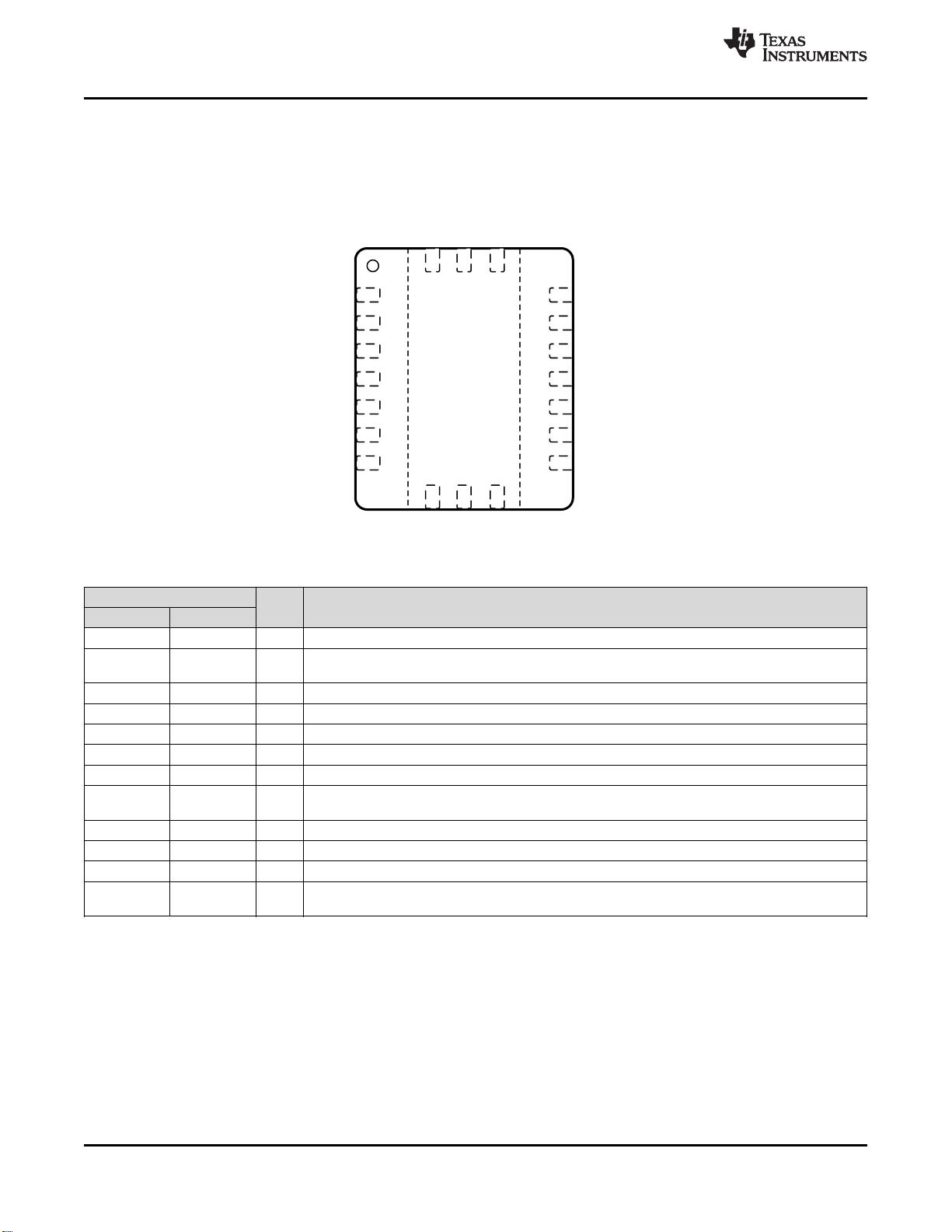
5 Pin Configuration and Functions
DSJ Package
14-Pin VSON with Exposed Thermal Pad
Top View
Pin Functions
PIN
I/O DESCRIPTION
NAME NO.
EN 12 I Enable input (1 enabled, 0 disabled), must not be left open
FB 3 I Voltage feedback of adjustable versions, must be connected to VOUT on fixed output voltage
versions
GND 2 – Control / logic ground
L1 8, 9 I Connection for inductor
L2 6, 7 I Connection for inductor
PG 14 O Output power good (1 good, 0 failure; open-drain), can be left open
PGND – Power ground
PS/SYNC 13 I Enable / disable power save mode (1 disabled, 0 enabled, clock signal for synchronization), must
not be left open
VIN 10, 11 I Supply voltage for power stage
VINA 1 I Supply voltage for control stage
VOUT 4, 5 O Buck-boost converter output
Exposed
Thermal Pad
–
The exposed thermal pad is connected to PGND.

5
TPS63020
,
TPS63021
www.ti.com.cn
ZHCSJG8I –JULY 2010–REVISED OCTOBER 2019
Copyright © 2010–2019, Texas Instruments Incorporated
(1) Stresses beyond those listed under Absolute Maximum Ratings may cause permanent damage to the device. These are stress ratings
only, and functional operation of the device at these or any other conditions beyond those indicated under Recommended Operating
Conditions is not implied. Exposure to absolute-maximum-rated conditions for extended periods my affect device reliability.
(2) All voltages are with respect to network ground terminal.
(3) Normal switching operation
6 Specifications
6.1 Absolute Maximum Ratings
over operating free-air temperature range (unless otherwise noted)
(1)
MIN MAX UNIT
Voltage
(2)
VIN, VINA, VOUT, PS/SYNC, EN, FB, PG –0.3 7 V
L1, L2 (DC) –0.3 7 V
L1, L2 (AC, less than 10 ns)
(3)
–3 10 V
Operating junction temperature, T
J
–40 150 °C
Storage temperature, T
stg
–65 150 °C
(1) JEDEC document JEP155 states that, with basic ESD control methods applied, 500 V HBM allows a safe manufacturing with proven
margin.
(2) JEDEC document JEP157 states that, with basic ESD control methods applied, 250 V CDM allows a safe manufacturing.
6.2 ESD Ratings
VALUE UNIT
V
(ESD)
Electrostatic discharge
Human body model (HBM), per ANSI/ESDA/JEDEC JS-001,
pins VIN, VINA, L1
(1)
±500
V
Human body model (HBM), per ANSI/ESDA/JEDEC JS-001,
all other pins
(1)
±2000
Charged device model (CDM), per JEDEC specification JESD22-C101,
all pins
(2)
±1500
6.3 Recommended Operating Conditions
MIN NOM MAX UNIT
Supply voltage at VIN, VINA 1.8 5.5 V
Operating free air temperature, T
A
–40 85 °C
Operating junction temperature, T
J
–40 125 °C
(1) For more information about traditional and new thermal metrics, see the Semiconductor and IC Package Thermal Metrics application
report.
6.4 Thermal Information
THERMAL METRIC
(1)
TPS6302x
UNITDSJ (VSON)
14 PINS
R
θJA
Junction-to-ambient thermal resistance 41.8 °C/W
R
θJC(top)
Junction-to-case (top) thermal resistance 47 °C/W
R
θJB
Junction-to-board thermal resistance 17 °C/W
ψ
JT
Junction-to-top characterization parameter 0.9 °C/W
ψ
JB
Junction-to-board characterization parameter 16.8 °C/W
R
θJC(bot)
Junction-to-case (bottom) thermal resistance 3.6 °C/W


评论1