没有合适的资源?快使用搜索试试~ 我知道了~
DRV832x 6 to 60V 3相MOS预驱 带3电流运放和1个BUCK1
需积分: 0 0 下载量 178 浏览量
2022-08-03
17:49:52
上传
评论
收藏 5.19MB PDF 举报
温馨提示
试读
94页
DRV832x 6 to 60V 3相MOS预驱 带3电流运放和1个BUCK1
资源详情
资源评论
资源推荐
6 to 60 V
DRV832x
Three-Phase
Smart Gate Driver
PWM
Gate Drive
Current
Sense
Current Sense
3x Sense Amplifiers
(DRV8323 only)
N-Channel
MOSFETs
nFAULT
M
SPI or H/W
600 mA
Protection
Controller
Buck Regulator
Copyright © 2017, Texas Instruments Incorporated
Product
Folder
Order
Now
Technical
Documents
Tools &
Software
Support &
Community
Reference
Design
An IMPORTANT NOTICE at the end of this data sheet addresses availability, warranty, changes, use in safety-critical applications,
intellectual property matters and other important disclaimers. PRODUCTION DATA.
DRV8320
,
DRV8320R
DRV8323
,
DRV8323R
SLVSDJ3C –FEBRUARY 2017–REVISED AUGUST 2018
DRV832x 6 to 60-V Three-Phase Smart Gate Driver
1
1 Features
1
• Triple Half-Bridge Gate Driver
– Drives 3 High-Side and 3 Low-Side N-Channel
MOSFETs (NMOS)
• Smart Gate Drive Architecture
– Adjustable Slew Rate Control
– 10-mA to 1-A Peak Source Current
– 20-mA to 2-A Peak Sink Current
• Integrated Gate Driver Power Supplies
– Supports 100% PWM Duty Cycle
– High-Side Charge Pump
– Low-Side Linear Regulator
• 6 to 60-V Operating Voltage Range
• Optional Integrated Buck Regulator
– LMR16006X SIMPLE SWITCHER
®
– 4 to 60-V Operating Voltage Range
– 0.8 to 60-V, 600-mA Output Capability
• Optional Integrated Triple Current Sense
Amplifiers (CSAs)
– Adjustable Gain (5, 10, 20, 40 V/V)
– Bidirectional or Unidirectional Support
• SPI and Hardware Interface Available
• 6x, 3x, 1x, and Independent PWM Modes
• Supports 1.8-V, 3.3-V, and 5-V Logic Inputs
• Low-Power Sleep Mode (12 µA)
• Linear Voltage Regulator, 3.3 V, 30 mA
• Compact QFN Packages and Footprints
• Efficient System Design With Power Blocks
• Integrated Protection Features
– VM Undervoltage Lockout (UVLO)
– Charge Pump Undervoltage (CPUV)
– MOSFET Overcurrent Protection (OCP)
– Gate Driver Fault (GDF)
– Thermal Warning and Shutdown (OTW/OTSD)
– Fault Condition Indicator (nFAULT)
2 Applications
• Brushless-DC (BLDC) Motor Modules and PMSM
• Fans, Pumps, and Servo Drives
• E-Bikes, E-Scooters, and E-Mobility
• Cordless Garden and Power Tools, Lawnmowers
• Cordless Vacuum Cleaners
• Drones, Robotics, and RC Toys
• Industrial and Logistics Robots
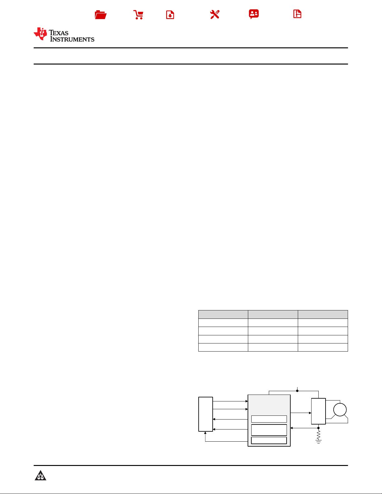
3 Description
The DRV832x family of devices is an integrated gate
driver for three-phase applications. The devices
provide three half-bridge gate drivers, each capable
of driving high-side and low-side N-channel power
MOSFETs. The DRV832x generates the correct gate
drive voltages using an integrated charge pump for
the high-side MOSFETs and a linear regulator for the
low-side MOSFETs. The Smart Gate Drive
architecture supports peak gate drive currents up to
1-A source and 2-A. The DRV832x can operate from
a single power supply and supports a wide input
supply range of 6 to 60 V for the gate driver and 4 to
60 V for the optional buck regulator.
The 6x, 3x, 1x, and independent input PWM modes
allow for simple interfacing to controller circuits. The
configuration settings for the gate driver and device
are highly configurable through the SPI or hardware
(H/W) interface. The DRV8323 and DRV8323R
devices integrate three low-side current sense
amplifiers that allow bidirectional current sensing on
all three phases of the drive stage. The DRV8320R
and DRV8323R devices integrate a 600-mA buck
regulator.
A low-power sleep mode is provided to achieve low
quiescent current draw by shutting down most of the
internal circuitry. Internal protection functions are
provided for undervoltage lockout, charge pump fault,
MOSFET overcurrent, MOSFET short circuit, gate
driver fault, and overtemperature. Fault conditions are
indicated on the nFAULT pin with details through the
device registers for SPI device variants.
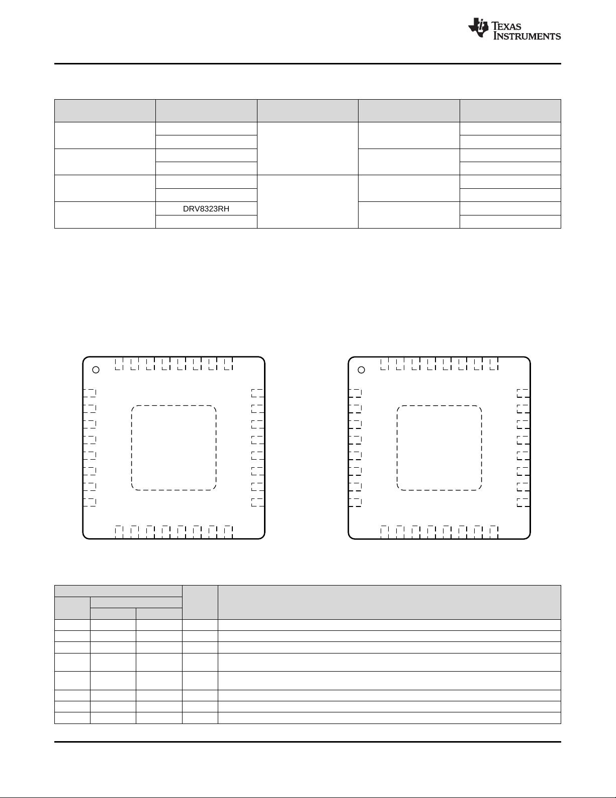
Device Information
(1)
PART NUMBER PACKAGE BODY SIZE (NOM)
DRV8320 WQFN (32) 5.00 mm × 5.00 mm
DRV8320R VQFN (40) 6.00 mm × 6.00 mm
DRV8323 WQFN (40) 6.00 mm × 6.00 mm
DRV8323R VQFN (48) 7.00 mm × 7.00 mm
(1) For all available packages, see the orderable addendum at
the end of the data sheet.
Simplified Schematic
2
DRV8320
,
DRV8320R
DRV8323
,
DRV8323R
SLVSDJ3C –FEBRUARY 2017–REVISED AUGUST 2018
www.ti.com
Product Folder Links: DRV8320 DRV8320R DRV8323 DRV8323R
Submit Documentation Feedback Copyright © 2017–2018, Texas Instruments Incorporated
Table of Contents
1 Features.................................................................. 1
2 Applications ........................................................... 1
3 Description ............................................................. 1
4 Revision History..................................................... 2
5 Device Comparison Table..................................... 4
6 Pin Configuration and Functions......................... 4
7 Specifications....................................................... 11
7.1 Absolute Maximum Ratings .................................... 11
7.2 ESD Ratings .......................................................... 11
7.3 Recommended Operating Conditions..................... 12
7.4 Thermal Information................................................ 12
7.5 Electrical Characteristics......................................... 13
7.6 SPI Timing Requirements ....................................... 18
7.7 Typical Characteristics............................................ 19
8 Detailed Description............................................ 21
8.1 Overview ................................................................. 21
8.2 Functional Block Diagram ....................................... 22
8.3 Feature Description................................................. 30
8.4 Device Functional Modes........................................ 50
8.5 Programming........................................................... 51
8.6 Register Maps......................................................... 53
9 Application and Implementation ........................ 61
9.1 Application Information............................................ 61
9.2 Typical Application ................................................. 61
10 Power Supply Recommendations ..................... 70
10.1 Bulk Capacitance Sizing ....................................... 70
11 Layout................................................................... 71
11.1 Layout Guidelines ................................................. 71
11.2 Layout Example .................................................... 72
12 Device and Documentation Support ................. 73
12.1 Device Support...................................................... 73
12.2 Documentation Support ........................................ 73
12.3 Related Links ........................................................ 73
12.4 Receiving Notification of Documentation Updates 74
12.5 Community Resources.......................................... 74
12.6 Trademarks........................................................... 74
12.7 Electrostatic Discharge Caution............................ 74
12.8 Glossary................................................................ 74
13 Mechanical, Packaging, and Orderable
Information ........................................................... 74
4 Revision History
NOTE: Page numbers for previous revisions may differ from page numbers in the current version.
Changes from Revision B (December 2017) to Revision C Page
• Changed the Applications....................................................................................................................................................... 1
• Updated input labels for the INLx and INHx signals in the Layout Example imags ............................................................. 72
• Added the DRV835x device options to the image in the Device Nomenclature section...................................................... 73
Changes from Revision A (April 2017) to Revision B Page
• Changed the low-power sleep mode supply current from the maximum value (20 µA) to the typical value (12 µA) in
the Features............................................................................................................................................................................ 1
• Changed the Applications....................................................................................................................................................... 1
• Changed the GAIN value from 45 kΩ to 47 kΩ in the test condition of the amplifier gain for the H/W device in the
Electrical Characteristics table ............................................................................................................................................. 15
• Deleted t
EN_nSCS
from the SPI Slave Mode Timing Diagram................................................................................................. 18
• Added a note to the Synchronous 1x PWM Mode to define !PWM ..................................................................................... 31
• Updated the Auto Offset Calibration section ........................................................................................................................ 44
• Updated the V
DS
Latched Shutdown and V
DS
Automatic Retry sections ............................................................................. 48
• Updated the Sleep Mode section ......................................................................................................................................... 50
• Changed the address listed in the title for the Gate Drive LS Register section to the correct register address, 0x04........ 58
• Changed the maximum Q
g
value for both trapezoidal and sinusoidal commutation the V
VM
= 8 V example of the
Detailed Design Procedure................................................................................................................................................... 63
• Changed I
DRIVEP
and I
DRIVEN
equations in the IDRIVE Configuration section ....................................................................... 64
3
DRV8320
,
DRV8320R
DRV8323
,
DRV8323R
www.ti.com
SLVSDJ3C –FEBRUARY 2017–REVISED AUGUST 2018
Product Folder Links: DRV8320 DRV8320R DRV8323 DRV8323R
Submit Documentation FeedbackCopyright © 2017–2018, Texas Instruments Incorporated
Changes from Original (February 2017) to Revision A Page
• Changed the test condition for the I
BIAS
parameter in the Electrical Characteristics table................................................... 16
• Changed the GHx values in the 3x PWM Mode Truth Table............................................................................................... 31
• Changed the calibration description and added auto calibration feature description .......................................................... 44
32 CPL9SLB
1CPH 24 DVDD
31 PGND10GLB
2VCP 23 AGND
30 INLC11SHB
3VM 22 ENABLE
29 INHC12GHB
4VDRAIN 21 nSCS
28 INLB13GHC
5GHA 20 SCLK
27 INHB14SHC
6SHA 19 SDI
26 INLA15GLC
7GLA 18 SDO
25 INHA16SLC
8SLA 17 nFAULT
Not to scale
Thermal
Pad
32 CPL9SLB
1CPH 24 DVDD
31 PGND10GLB
2VCP 23 AGND
30 INLC11SHB
3VM 22 ENABLE
29 INHC12GHB
4VDRAIN 21 NC
28 INLB13GHC
5GHA 20 VDS
27 INHB14SHC
6SHA 19 IDRIVE
26 INLA15GLC
7GLA 18 MODE
25 INHA16SLC
8SLA 17 nFAULT
Not to scale
Thermal
Pad
4
DRV8320
,
DRV8320R
DRV8323
,
DRV8323R
SLVSDJ3C –FEBRUARY 2017–REVISED AUGUST 2018
www.ti.com
Product Folder Links: DRV8320 DRV8320R DRV8323 DRV8323R
Submit Documentation Feedback Copyright © 2017–2018, Texas Instruments Incorporated
(1) For more information on the device name and device options, see the Device Nomenclature section. For additional details, see the
Architecture for Brushless-DC Gate Drive Systems application report.
5 Device Comparison Table
DEVICE VARIANT
(1)
CURRENT SENSE
AMPLIFIERS
BUCK REGULATOR
(1)
INTERFACE
(1)
DRV8320
DRV8320H
0
None
Hardware
DRV8320S SPI
DRV8320R
DRV8320RH
600 mA
Hardware
DRV8320RS SPI
DRV8323
DRV8323H
3
None
Hardware
DRV8323S SPI
DRV8323R
DRV8323RH
600 mA
Hardware
DRV8323RS SPI
6 Pin Configuration and Functions
DRV8320H RTV Package
32-Pin WQFN With Exposed Thermal Pad
Top View
DRV8320S RTV Package
32-Pin WQFN With Exposed Thermal Pad
Top View
(1) PWR = power, I = input, O = output, NC = no connection, OD = open-drain output
Pin Functions —32-Pin DRV8320 Devices
PIN
TYPE
(1)
DESCRIPTION
NAME
NO.
DRV8320H DRV8320S
AGND 23 23 PWR Device analog ground. Connect to system ground.
CPH 1 1 PWR Charge pump switching node. Connect a X5R or X7R, 47-nF, VM-rated ceramic capacitor between the CPH and CPL pins.
CPL 32 32 PWR Charge pump switching node. Connect a X5R or X7R, 47-nF, VM-rated ceramic capacitor between the CPH and CPL pins.
DVDD 24 24 PWR
3.3-V internal regulator output. Connect a X5R or X7R, 1-µF, 6.3-V ceramic capacitor between the DVDD and AGND pins.
This regulator can source up to 30 mA externally.
ENABLE 22 22 I
Gate driver enable. When this pin is logic low the device goes to a low-power sleep mode. An 8 to 40-µs pulse can be used
to reset fault conditions.
GHA 5 5 O High-side gate driver output. Connect to the gate of the high-side power MOSFET.
GHB 12 12 O High-side gate driver output. Connect to the gate of the high-side power MOSFET.
GHC 13 13 O High-side gate driver output. Connect to the gate of the high-side power MOSFET.
5
DRV8320
,
DRV8320R
DRV8323
,
DRV8323R
www.ti.com
SLVSDJ3C –FEBRUARY 2017–REVISED AUGUST 2018
Product Folder Links: DRV8320 DRV8320R DRV8323 DRV8323R
Submit Documentation FeedbackCopyright © 2017–2018, Texas Instruments Incorporated
Pin Functions —32-Pin DRV8320 Devices (continued)
PIN
TYPE
(1)
DESCRIPTION
NAME
NO.
DRV8320H DRV8320S
GLA 7 7 O Low-side gate driver output. Connect to the gate of the low-side power MOSFET.
GLB 10 10 O Low-side gate driver output. Connect to the gate of the low-side power MOSFET.
GLC 15 15 O Low-side gate driver output. Connect to the gate of the low-side power MOSFET.
IDRIVE 19 — I Gate drive output current setting. This pin is a 7 level input pin set by an external resistor.
INHA 25 25 I High-side gate driver control input. This pin controls the output of the high-side gate driver.
INHB 27 27 I High-side gate driver control input. This pin controls the output of the high-side gate driver.
INHC 29 29 I High-side gate driver control input. This pin controls the output of the high-side gate driver.
INLA 26 26 I Low-side gate driver control input. This pin controls the output of the low-side gate driver.
INLB 28 28 I Low-side gate driver control input. This pin controls the output of the low-side gate driver.
INLC 30 30 I Low-side gate driver control input. This pin controls the output of the low-side gate driver.
MODE 18 — I PWM input mode setting. This pin is a 4 level input pin set by an external resistor.
NC 21 — NC No internal connection. This pin can be left floating or connected to system ground.
nFAULT 17 17 OD Fault indicator output. This pin is pulled logic low during a fault condition and requires an external pullup resistor.
nSCS — 21 I Serial chip select. A logic low on this pin enables serial interface communication.
PGND 31 31 PWR Device power ground. Connect to system ground.
SCLK — 20 I Serial clock input. Serial data is shifted out and captured on the corresponding rising and falling edge on this pin.
SDI — 19 I Serial data input. Data is captured on the falling edge of the SCLK pin.
SDO — 18 OD Serial data output. Data is shifted out on the rising edge of the SCLK pin. This pin requires an external pullup resistor.
SHA 6 6 I High-side source sense input. Connect to the high-side power MOSFET source.
SHB 11 11 I High-side source sense input. Connect to the high-side power MOSFET source.
SHC 14 14 I High-side source sense input. Connect to the high-side power MOSFET source.
SLA 8 8 I Low-side source sense input. Connect to the low-side power MOSFET source.
SLB 9 9 I Low-side source sense input. Connect to the low-side power MOSFET source.
SLC 16 16 I Low-side source sense input. Connect to the low-side power MOSFET source.
VCP 2 2 PWR Charge pump output. Connect a X5R or X7R, 1-µF, 16-V ceramic capacitor between the VCP and VM pins.
VDRAIN 4 4 I High-side MOSFET drain sense input. Connect to the common point of the MOSFET drains.
VDS 20 — I VDS monitor trip point setting. This pin is a 7 level input pin set by an external resistor.
VM 3 3 PWR
Gate driver power supply input. Connect to the bridge power supply. Connect a X5R or X7R, 0.1-µF, VM-rated ceramic and
greater then or equal to 10-uF local capacitance between the VM and PGND pins.
Thermal Pad PWR Must be connected to ground
剩余93页未读,继续阅读
WaiyuetFung
- 粉丝: 63
- 资源: 316
上传资源 快速赚钱
- 我的内容管理 展开
- 我的资源 快来上传第一个资源
- 我的收益 登录查看自己的收益
- 我的积分 登录查看自己的积分
- 我的C币 登录后查看C币余额
- 我的收藏
- 我的下载
- 下载帮助
安全验证
文档复制为VIP权益,开通VIP直接复制
信息提交成功
评论0