没有合适的资源?快使用搜索试试~ 我知道了~
drv8302 60V 三相MOS预驱 2路电流运放+1个BUCK1
需积分: 0 6 下载量 89 浏览量
2022-08-03
18:04:12
上传
评论
收藏 905KB PDF 举报
温馨提示
试读
33页
drv8302 60V 三相MOS预驱 2路电流运放+1个BUCK1
资源详情
资源评论
资源推荐
DRV8302
PWM
8 to 60 V
MCU
N-Channel
MOSFETs
Gate Drive
Sense
3-Phase
Brushless
Gate
Driver
Buck
Converter
HW Control
nFAULT
nOCTW
Vcc (Buck)
Diff Amps
M
Product
Folder
Sample &
Buy
Technical
Documents
Tools &
Software
Support &
Community
An IMPORTANT NOTICE at the end of this data sheet addresses availability, warranty, changes, use in safety-critical applications,
intellectual property matters and other important disclaimers. PRODUCTION DATA.
English Data Sheet: SLES267
DRV8302
ZHCS138C –AUGUST 2011–REVISED MARCH 2016
DRV8302 具具有有双双路路分分流流放放大大器器和和
降降压压稳稳压压器器的的三三相相栅栅极极驱驱动动器器 – 硬硬件件控控制制
1
1 特特性性
1
• 8V 至 60V 运行电源电压范围
• 栅极可驱动 1.7A 拉电流和 2.3A 灌电流
• 支持 100% 占空比的自举栅极驱动器
• 6 种或 3 种脉宽调制 (PWM) 输入模式
• 两个增益和偏移可调节的集成分流放大器
• 支持 3.3V 和 5V 接口
• 硬件控制接口
• 保护 特性:
– 可编程死区控制 (DTC)
– 可编程过流保护 (OCP)
– PVDD 和 GVDD 欠压锁定 (UVLO)
– GVDD 过压锁定 (OVLO)
– 过热警告/关断 (OTW/OTS)
– 通过 nFAULT 和 nOCTW 引脚报告
2 应应用用范范围围
• 三相无刷直流 (BLDC) 电机和永磁同步电机
(PMSM)
• 持续正压通气 (CPAP) 和泵
• 电动自行车
• 电动工具
• 机器人和遥控 (RC) 玩具
• 工业自动化
3 说说明明
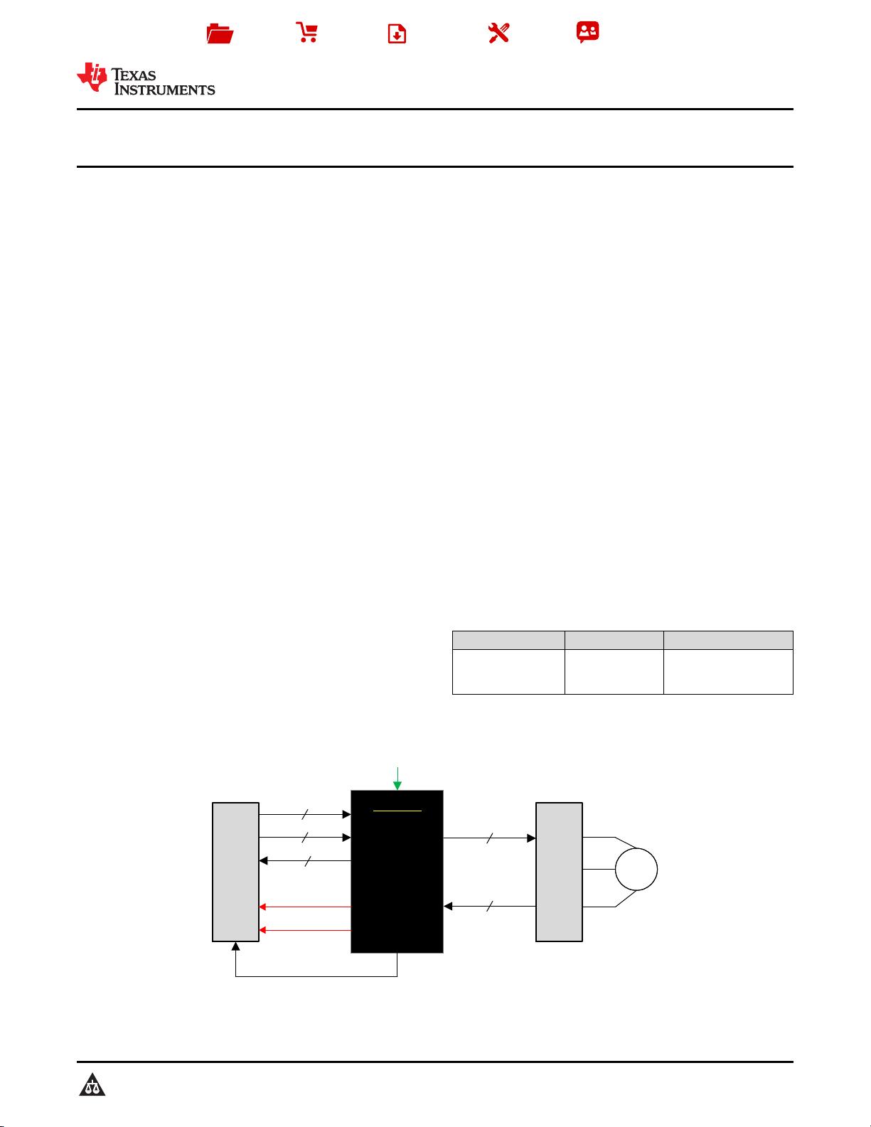
DRV8302 是一款适用于三相电机驱动应用的栅极驱动
器集成 电路 (IC)。它提供三个半桥驱动器,每个半桥
驱动器可驱动两个 N 沟道金属氧化物半导体场效应晶
体管 (MOSFET)。该器件最高支持 1.7A 拉电流和
2.3A 峰值电流。DRV8302 可通过具有 8V 至 60V 宽
工作电压范围的单一电源供电。它采用自举栅极驱动器
架构和涓流充电电路来支持 100% 占空比。DRV8302
在切换高侧或低侧 MOSFET 时使用自动握手机制,以
防止发生电流击穿。高侧和低侧 MOSFET 的集成
VDS 感测用于防止外部功率级出现过流现象。
DRV8303 具备两个对电流进行精确测量的分流放大
器。这两个放大器支持双向电流感测,最高可提供 3V
可调节输出偏移。
DRV8302 还包括输出和开关频率可调节的集成开关模
式降压转换器。该降压转换器最高可提供 1.5A 的电
流,以满足 MCU 或其他系统的功率需求。
凭借硬件接口可配置不同器件参数,包括死区、过流、
PWM 模式和放大器设置。错误条件通过 nFAULT 和
nOCTW 引脚报告。
器器件件信信息息
(1)
器器件件型型号号 封封装装 封封装装尺尺寸寸((标标称称值值))
DRV8302
带散热片薄型小
外形尺寸封装
(HTSSOP) (56)
14.00mm x 6.10mm
(1) 要了解所有可用封装,请见数据表末尾的可订购产品附录。
简简化化电电路路原原理理图图
2
DRV8302
ZHCS138C –AUGUST 2011–REVISED MARCH 2016
www.ti.com.cn
Copyright © 2011–2016, Texas Instruments Incorporated
目目录录
1 特特性性.......................................................................... 1
2 应应用用范范围围................................................................... 1
3 说说明明.......................................................................... 1
4 修修订订历历史史记记录录 ........................................................... 2
5 Pin Configuration and Functions......................... 3
6 Specifications......................................................... 5
6.1 Absolute Maximum Ratings ...................................... 5
6.2 ESD Ratings.............................................................. 5
6.3 Recommended Operating Conditions....................... 6
6.4 Thermal Information.................................................. 6
6.5 Electrical Characteristics........................................... 7
6.6 Gate Timing and Protection Characteristics ............. 8
6.7 Current Shunt Amplifier Characteristics.................... 8
6.8 Buck Converter Characteristics ................................ 9
6.9 Typical Characteristics............................................ 10
7 Detailed Description............................................ 11
7.1 Overview ................................................................. 11
7.2 Function Block Diagram.......................................... 12
7.3 Feature Description................................................. 13
7.4 Device Functional Modes........................................ 19
8 Application and Implementation ........................ 20
8.1 Application Information............................................ 20
8.2 Typical Application ................................................. 21
9 Power Supply Recommendations...................... 24
9.1 Bulk Capacitance .................................................... 24
10 Layout................................................................... 25
10.1 Layout Guidelines ................................................. 25
10.2 Layout Example .................................................... 25
11 器器件件和和文文档档支支持持 ..................................................... 26
11.1 文档支持................................................................ 26
11.2 社区资源................................................................ 26
11.3 商标 ....................................................................... 26
11.4 静电放电警告......................................................... 26
11.5 Glossary................................................................ 26
12 机机械械、、封封装装和和可可订订购购信信息息....................................... 26
4 修修订订历历史史记记录录
注:之前版本的页码可能与当前版本有所不同。
Changes from Revision B (February 2016) to Revision C Page
• 已删除 REG 0x02 from the test conditions of the I
oso1
and I
osi1
parameters in the Electrical Characteristics table .............. 7
• 已更改 the value of R1 + R2 ≥ 100 KΩ to R1 + R2 ≥ 1 KΩ in the OC_ADJ section............................................................ 17
Changes from Revision A (December 2015) to Revision B Page
• Changed VEN_BUCK in Buck Converter Characteristics From: MIN = 0.9 V and MAX = 1.55 V To: MIN = 1.11 V
and MAX = 1.36 V. ................................................................................................................................................................ 9
Changes from Original (August 2011) to Revision A Page
• 已添加
引脚配置和功能
部分,ESD
额定值
表,
特性 描述
部分,
器件功能模式
,
应用和实施
部分,
电源相关建议
部
分,
布局
部分,
器件和文档支持
部分以及
机械、封装和可订购信息
部分 ................................................................................ 1
• V
PVDD
absolute max voltage rating reduced from 70 V to 65 V ............................................................................................. 5
• Clarification made on how the OCP status bits report in Overcurrent Protection (OCP) and Reporting ............................ 16
• Update to PVDD1 undervoltage protection in Undervoltage Protection (UVLO) describing specific transient brownout
issue. ................................................................................................................................................................................... 17
• Update to EN_GATE pin functional description in EN_GATE clarifying proper EN_GATE reset pulse lengths. ................ 19
• Added gate driver power-up sequencing errata Gate Driver Power Up Sequencing Errdata.............................................. 20
• Added Community Resources ............................................................................................................................................. 24
1
RT_CLK
2
3
4
12
5
6
7
8
9
10
11
13
14
15
16
17
18
26
19
20
21
22
23
24
25
27
28
56
55
54
53
45
52
51
50
49
48
47
46
44
43
42
41
40
39
31
38
37
36
35
34
33
32
30
29
COMP
VSENSE
PWRGD
nOCTW
nFAULT
DTC
M_PWM
M_OC
DC_CAL
GAIN
OC_ADJ
GVDD
CP1
CP2
EN_GATE
INH_A
INL_A
INH_B
INL_B
INH_C
INL_C
DVDD
REF
SO1
SO2
AVDD
AGND
SS_TR
EN_BUCK
PVDD2
PVDD2
BST_BK
PH
PH
BIAS
BST_A
GL_A
GH_A
SH_A
SL_A
BST_B
GH_B
SH_B
GL_B
SL_B
BST_C
GH_C
SH_C
GL_C
SL_C
SN1
SP1
SN2
SP2
PVDD1
GND (57) - PowerPAD
3
DRV8302
www.ti.com.cn
ZHCS138C –AUGUST 2011–REVISED MARCH 2016
Copyright © 2011–2016, Texas Instruments Incorporated
(1) KEY: I =Input, O = Output, P = Power
5 Pin Configuration and Functions
DCA Package
56-Pin HTSSOP With PowerPAD™
Top View
Pin Functions
PIN
I/O
(1)
DESCRIPTION
NO. NAME
1 RT_CLK I
Resistor timing and external clock for buck regulator. Resistor should connect to GND (PowerPAD™)
with very short trace to reduce the potential clock jitter due to noise.
2 COMP O Buck error amplifier output and input to the output switch current comparator.
3 VSENSE I Buck output voltage sense pin. Inverting node of error amplifier.
4 PWRGD I
An open drain output with external pullup resistor required. Asserts low if buck output voltage is low
due to thermal shutdown, dropout, overvoltage, or EN_BUCK shut down
5 nOCTW O
Overcurrent and overtemperature warning indicator. This output is open drain with external pullup
resistor required.
6 nFAULT O Fault report indicator. This output is open drain with external pullup resistor required.
7 DTC I Dead-time adjustment with external resistor to GND
8 M_PWM I
Mode selection pin for PWM input configuration. If M_PWM = LOW, the device supports 6 independent
PWM inputs. When M_PWM = HIGH, the device must be connected to ONLY 3 PWM input signals on
INH_x. The complementary PWM signals for low side signaling will be internally generated from the
high side inputs.
9 M_OC I
Mode selection pin for over-current protection options. If M_OC = LOW, the gate driver will operate in a
cycle-by-cycle current limiting mode. If M_OC = HIGH, the gate driver will shutdown the channel which
detected an over-current event.
10 GAIN O
Gain selection for integrated current shunt amplifiers. If GAIN = LOW, the internal current shunt
amplifiers have a gain of 10V/V. If GAIN = HIGH, the current shunt amplifiers have a gain of 40V/V.
11 OC_ADJ I
Overcurrent trip set pin. Apply a voltage on this pin to set the trip point for the internal overcurrent
protection circuitry. A voltage divider from DVDD is recommended.
12 DC_CAL I
When DC_CAL is high, device shorts inputs of shunt amplifiers and disconnects loads. DC offset
calibration can be done through external microcontroller.
这个脚为高时关闭电流传感运放供
MCU的AD自校准。
过流比较电压的设置
4
DRV8302
ZHCS138C –AUGUST 2011–REVISED MARCH 2016
www.ti.com.cn
Copyright © 2011–2016, Texas Instruments Incorporated
Pin Functions (continued)
PIN
I/O
(1)
DESCRIPTION
NO. NAME
13 GVDD P Internal gate driver voltage regulator. GVDD cap should connect to GND
14 CP1 P Charge pump pin 1, ceramic cap should be used between CP1 and CP2
15 CP2 P Charge pump pin 2, ceramic cap should be used between CP1 and CP2
16 EN_GATE I Enable gate driver and current shunt amplifiers. Control buck via EN_BUCK pin.
17 INH_A I PWM Input signal (high side), half-bridge A
18 INL_A I PWM Input signal (low side), half-bridge A
19 INH_B I PWM Input signal (high side), half-bridge B
20 INL_B I PWM Input signal (low side), half-bridge B
21 INH_C I PWM Input signal (high side), half-bridge C
22 INL_C I PWM Input signal (low side), half-bridge C
23 DVDD P
Internal 3.3-V supply voltage. DVDD cap should connect to AGND. This is an output, but not specified
to drive external circuitry.
24 REF I
Reference voltage to set output of shunt amplfiiers with a bias voltage which equals to half of the
voltage set on this pin. Connect to ADC reference in microcontroller.
25 SO1 O Output of current amplifier 1
26 SO2 O Output of current amplifier 2
27 AVDD P
Internal 6-V supply voltage, AVDD cap should connect to AGND. This is an output, but not specified to
drive external circuitry.
28 AGND P Analog ground pin
29 PVDD1 P
Power supply pin for gate driver and current shunt amplifier. PVDD1 is independent of buck power
supply, PVDD2. PVDD1 cap should connect to GND
30 SP2 I
Input of current amplifier 2 (connecting to positive input of amplifier). Recommend to connect to ground
side of the sense resistor for the best commom mode rejection.
31 SN2 I Input of current amplifier 2 (connecting to negative input of amplifier).
32 SP1 I
Input of current amplifier 1 (connecting to positive input of amplifier). Recommend to connect to ground
side of the sense resistor for the best commom mode rejection.
33 SN1 I Input of current amplifier 1 (connecting to negative input of amplifier).
34 SL_C I
Low-Side MOSFET source connection, half-bridge C. Low-side V
DS
measured between this pin and
SH_C.
35 GL_C O Gate drive output for Low-Side MOSFET, half-bridge C
36 SH_C I
High-Side MOSFET source connection, half-bridge C. High-side V
DS
measured between this pin and
PVDD1.
37 GH_C O Gate drive output for High-Side MOSFET, half-bridge C
38 BST_C P Bootstrap cap pin for half-bridge C
39 SL_B I
Low-Side MOSFET source connection, half-bridge B. Low-side V
DS
measured between this pin and
SH_B.
40 GL_B O Gate drive output for Low-Side MOSFET, half-bridge B
41 SH_B I
High-Side MOSFET source connection, half-bridge B. High-side V
DS
measured between this pin and
PVDD1.
42 GH_B O Gate drive output for High-Side MOSFET, half-bridge B
43 BST_B P Bootstrap cap pin for half-bridge B
44 SL_A I
Low-Side MOSFET source connection, half-bridge A. Low-side V
DS
measured between this pin and
SH_A.
45 GL_A O Gate drive output for Low-Side MOSFET, half-bridge A
46 SH_A I
High-Side MOSFET source connection, half-bridge A. High-side V
DS
measured between this pin and
PVDD1.
47 GH_A O Gate drive output for High-Side MOSFET, half-bridge A
48 BST_A P Bootstrap cap pin for half-bridge A
49 BIAS I Bias pin. Connect 1M-Ω resistor to GND, or 0.1 µF capacitor to GND.
50, 51 PH O The source of the internal high side MOSFET of buck converter
MOS Gate Vcc,MOS的预驱电压输
出。其正常工作时在11.5V左右。
内部产生的,不要用于外部供电。
电流传感运放的偏置电压为此脚电压
的一般,外部在此脚输入外部ADC的
参考电压即可。
可用MCU控制,高电平(大于2V)开启,低电平时低于0.8V关闭
5
DRV8302
www.ti.com.cn
ZHCS138C –AUGUST 2011–REVISED MARCH 2016
Copyright © 2011–2016, Texas Instruments Incorporated
Pin Functions (continued)
PIN
I/O
(1)
DESCRIPTION
NO. NAME
52 BST_BK P Bootstrap cap pin for buck converter
53, 54 PVDD2 P Power supply pin for buck converter, PVDD2 cap should connect to GND.
55 EN_BUCK I
Enable buck converter. Internal pullup current source. Pull below 1.2 V to disable. Float to enable.
Adjust the input undervoltage lockout with two resistors
56 SS_TR I
Buck soft-start and tracking. An external capacitor connected to this pin sets the output rise time. Since
the voltage on this pin overrides the internal reference, it can be used for tracking and sequencing. Cap
should connect to GND
57
GND
(PWR_PAD)
P
GND pin. The exposed power pad must be electrically connected to ground plane through soldering to
PCB for proper operation and connected to bottom side of PCB through vias for better thermal
spreading.
(1) Stresses beyond those listed under Absolute Maximum Ratings may cause permanent damage to the device. These are stress ratings
only, which do not imply functional operation of the device at these or any other conditions beyond those indicated under Recommended
Operating Conditions. Exposure to absolute-maximum-rated conditions for extended periods may affect device reliability.
6 Specifications
6.1 Absolute Maximum Ratings
over operating free-air temperature range (unless otherwise noted)
(1)
MIN MAX UNIT
V
PVDD
Supply voltage Relative to PGND –0.3 65 V
PVDD
RAMP
Maximum supply voltage ramp rate Voltage rising up to PVDD
MAX
1 V/µs
V
PGND
Maximum voltage between PGND and GND –0.3 0.3 V
I
IN_MAX
Maximum current, all digital and analog input pins except nFAULT and nOCTW pins –1 1 mA
I
IN_OD_MAX
Maximum sinking current for open-drain pins (nFAULT and nOCTW Pins) 7 mA
V
OPA_IN
Voltage range for SPx and SNx pins –0.6 0.6 V
V
LOGIC
Input voltage range for logic/digital pins (INH_A, INL_A, INH_B, INL_B, INH_C, INL_C,
EN_GATE, M_PWM, M_OC, OC_ADJ, GAIN, DC_CAL)
–0.3 7 V
V
GVDD
Maximum voltage for GVDD pin 13.2 V
V
AVDD
Maximum voltage for AVDD pin 8 V
V
DVDD
Maximum voltage for DVDD pin 3.6 V
V
REF
Maximum reference voltage for current amplifier 7 V
I
REF
Maximum current for REF Pin 100 µA
T
J
Maximum operating junction temperature –40 150 °C
T
stg
Storage temperature –55 150 °C
(1) JEDEC document JEP155 states that 500-V HBM allows safe manufacturing with a standard ESD control process.
(2) JEDEC document JEP157 states that 250-V CDM allows safe manufacturing with a standard ESD control process.
6.2 ESD Ratings
VALUE UNIT
V
(ESD)
Electrostatic
discharge
Human-body model (HBM), per ANSI/ESDA/JEDEC JS-001
(1)
±2000
V
Charged-device model (CDM), per JEDEC specification JESD22-C101
(2)
±500
可用两个电阻对输入电压做分压,如
果欠压则关闭 BUCK,进而关闭MCU,
进而关闭 DRV8302 和 MOS预驱
BUCK和GATE预驱是
独立工作的
剩余32页未读,继续阅读
Xhinking
- 粉丝: 24
- 资源: 320
上传资源 快速赚钱
- 我的内容管理 展开
- 我的资源 快来上传第一个资源
- 我的收益 登录查看自己的收益
- 我的积分 登录查看自己的积分
- 我的C币 登录后查看C币余额
- 我的收藏
- 我的下载
- 下载帮助
安全验证
文档复制为VIP权益,开通VIP直接复制
信息提交成功
评论0