drv8313 内置MOS 2.5A 60V 3PWM1
需积分: 0 160 浏览量
2022-08-03
17:42:37
上传
评论
收藏 2.32MB PDF 举报

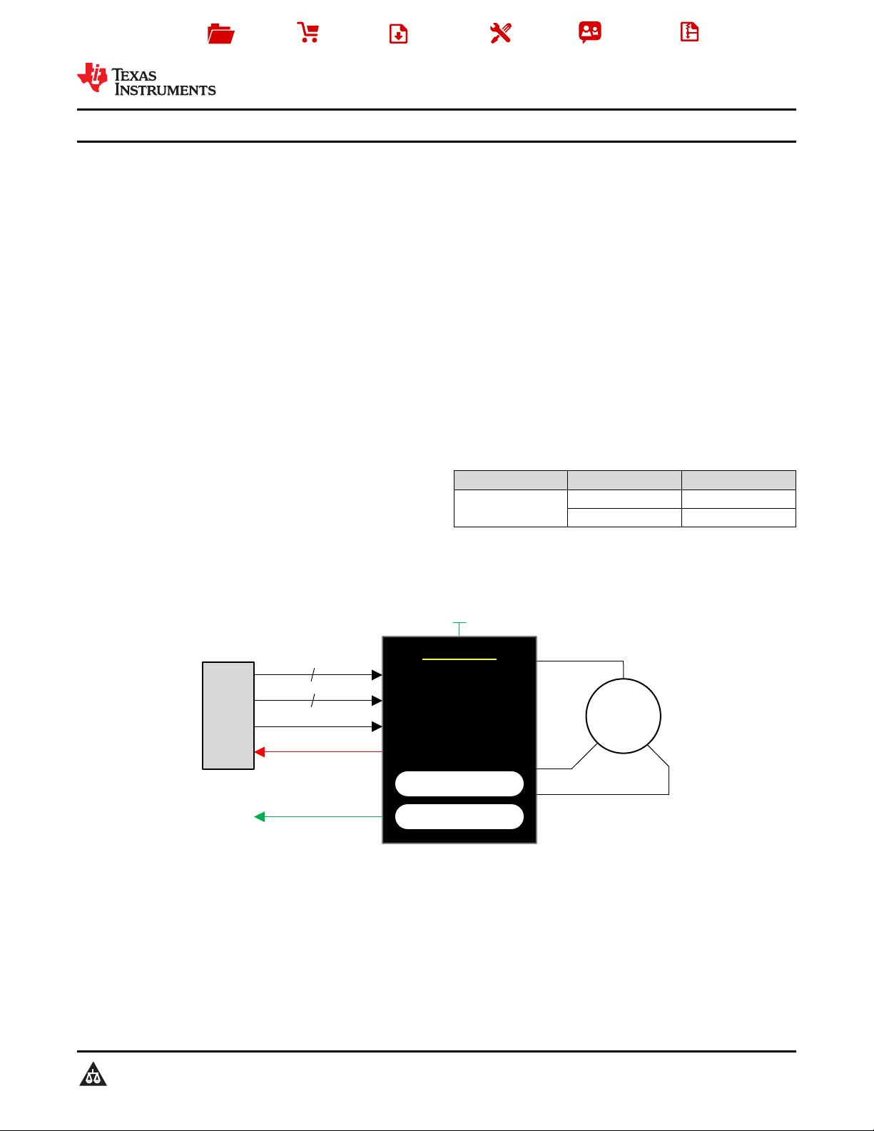
8 to 60 V
DRV8313
3 ½-H Bridge
Driver
IN
EN
Built-In Protection
nFAULT
M
3.3-V LDO
Controller
3.3 V
10 mA
nSLEEP
3.5 A
Copyright © 2016, Texas Instruments Incorporated
Product
Folder
Sample &
Buy
Technical
Documents
Tools &
Software
Support &
Community
Reference
Design
An IMPORTANT NOTICE at the end of this data sheet addresses availability, warranty, changes, use in safety-critical applications,
intellectual property matters and other important disclaimers. PRODUCTION DATA.
DRV8313
SLVSBA5D –OCTOBER 2012–REVISED APRIL 2016
DRV8313 2.5-A Triple 1/2-H Bridge Driver
1
1 Features
1
• Triple 1/2-H Bridge Driver IC
– 3-Phase brushless DC Motors
– Solenoid and Brushed DC Motors
• High Current-Drive Capability: 2.5-A Peak
• Low MOSFET ON-Resistance
• Independent 1/2-H-Bridge Control
• Uncommitted Comparator Can Be Used for
Current Limit or Other Functions
• Built-In 3.3-V 10-mA LDO Regulator
• 8-V to 60-V Operating Supply-Voltage Range
• Sleep Mode for Standby Operation
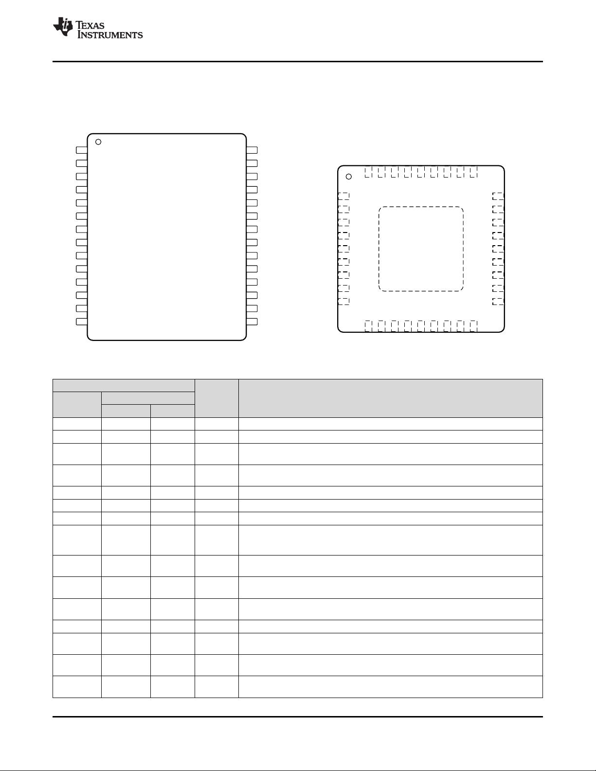
• Small Package and Footprint
– 28-Pin HTSSOP (PowerPAD™ Package)
– 36-Pin VQFN
2 Applications
• Camera Gimbals
• HVAC Motors
• Office Automation Machines
• Factory Automation and Robotics
3 Description
The DRV8313 provides three individually controllable
half-H-bridge drivers. The device is intended to drive
a three-phase brushless-DC motor, although it can
also be used to drive solenoids or other loads. Each
output driver channel consists of N-channel power
MOSFETs configured in a 1/2-H-bridge configuration.
Each 1/2-H-bridge driver has a dedicated ground
terminal, which allows independent external current
sensing.
An uncommitted comparator is integrated into the
DRV8313, which allows for the construction of
current-limit circuitry or other functions.
Internal protection functions are provided for
undervoltage, charge pump faults, overcurrent, short
circuits, and overtemperature. Fault conditions are
indicated by the nFAULT pin.
Device Information
(1)
PART NUMBER PACKAGE BODY SIZE (NOM)
DRV8313
HTSSOP (28) 9.70 mm × 4.40 mm
VQFN (36) 6.00 mm × 6.00 mm
(1) For all available packages, see the orderable addendum at
the end of the data sheet.
Simplified Schematic

剩余38页未读,继续阅读
资源评论


