QM77040 data sheet
需积分: 10 73 浏览量
2022-11-30
14:51:31
上传
评论
收藏 1.45MB PDF 举报

QM77040
Linear Multi-Mode Mid and High Band S-PAD for 3G/4G/5G Applications
QM77040 DS20190920 | Subject to change without notice
1 of 40
www.qorvo.com
Product Overview
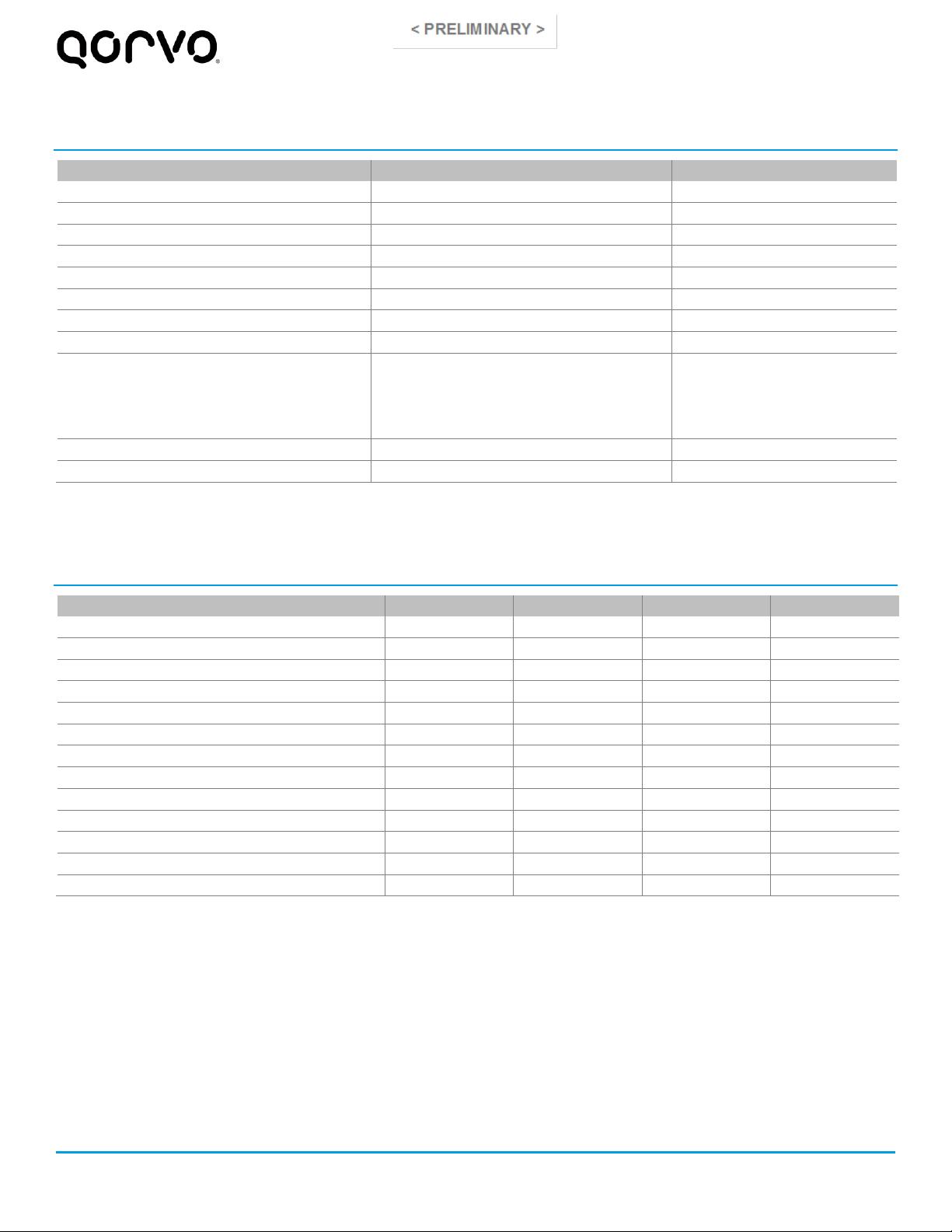
The Qorvo
®
QM77040 is a multi-mode, high efficiency linear
Mid Band and High Band S-PAD (Switched PA plus Duplexer)
module designed for use as the integrated RF front-end in
multi-mode WCDMA/CDMA/TDS-CDMA/LTE/NR mobile
cellular equipment. The high efficiency S-PAD contains two
amplifier paths for 3G/4G/5G Mid and High Band frequencies
followed by distribution switches, filters/duplexers/quadplexer
and antenna switches for multi-band coverage of both transmit
and receive functions. QM77040 band select and bias are
programmed through two Mobile Industry Processor Interface
(MIPI) buses. The QM77040 transmit-receive module supports
Average Power Tracking (APT) for higher system efficiency at
various power levels and modulations, as well as Envelope
Tracking (ET) for current consumption optimization.
The QM77040 is packaged in a RoHS-compliant, compact
62-pin, 6.5 x 8.6 x 0.8 (max) mm surface-mount leadless
package.
Functional Block Diagram
Functional Block Diagram
62 Pin 6.5x8.6 mm leadless SMT Package
Key Features
• Multi-Mode and Multi Band Capabilities;
WCDMA/CDMA2000/ FDD-LTE/TDD-LTE/NR
• Integrated Band 1, 2, 3, 4, 7, 34, 39, 40 and 41(38) with
Filters, Duplexers and Quadplexer for Transmit and Receive
• Additional Mid Bands Through External AUX Path
• Inter-band Downlink Carrier Aggregation (DL CA): B1+B3,
B39+B41, B3+B7, B1+B3+B7 and B3+B41
• Designed and Optimized for Use with DC-DC Converter
• Support of Average Power Tracking (APT) and Envelope
Tracking (ET) for High System Efficiency and Performance
• Support Power Class 2 (i.e. HPUE) for B41
• Support 5G NR for n41, n3 and n1
• MIPI RFFE 2.1 Applications
Applications
• 3G/4G/5G Multi-Mode Handsets
• WCDMA and LTE Datacards or Wearable Devices
• High Performance Communication Systems
• LTE Single Carrier Channel Bandwidths up to 20MHz and
5G NR Channel Bandwidths up to 100MHz
• LTE CA Bandwidths up to 60MHz, 16QAM and 64QAM
Ordering Information
Part Number
Description
QM77040SR
7” Reel with 100 pieces
QM77040TR13
13” Reel with 5000 pieces
QM77040DK
Design Kit
(includes Evaluation board)


剩余39页未读,继续阅读
资源评论


