FDB2532_FDP2532_FDI2532-芯片资料介绍.pdf
版权申诉
74 浏览量
2022-07-04
10:04:30
上传
评论
收藏 304KB PDF 举报

©2002 Fairchild Semiconductor Corporation
June 2002
FDB2532 / FDP2532 / FDI2532 Rev. A1
FDB2532 / FDP2532 / FDI2532
FDB2532 / FDP2532 / FDI2532
N-Channel PowerTrench
®
MOSFET
150V, 79A, 16mΩ
Features
•r
DS(ON)
= 14mΩ (Typ.), V
GS
= 10V, I
D
= 33A
•Q
g
(tot) = 86nC (Typ.), V
GS
= 10V
• Low Miller Charge
•Low Q
RR
Body Diode
• UIS Capability (Single Pulse and Repetitive Pulse)
• Qualified to AEC Q101
Formerly developmental type 82884
Applications
• DC/DC converters and Off-Line UPS
• Distributed Power Architectures and VRMs
• Primary Switch for 24V and 48V Systems
• High Voltage Synchronous Rectifier
• Direct Injection / Diesel Injection System
• 42V Automotive Load Control
• Electronic Valve Train System
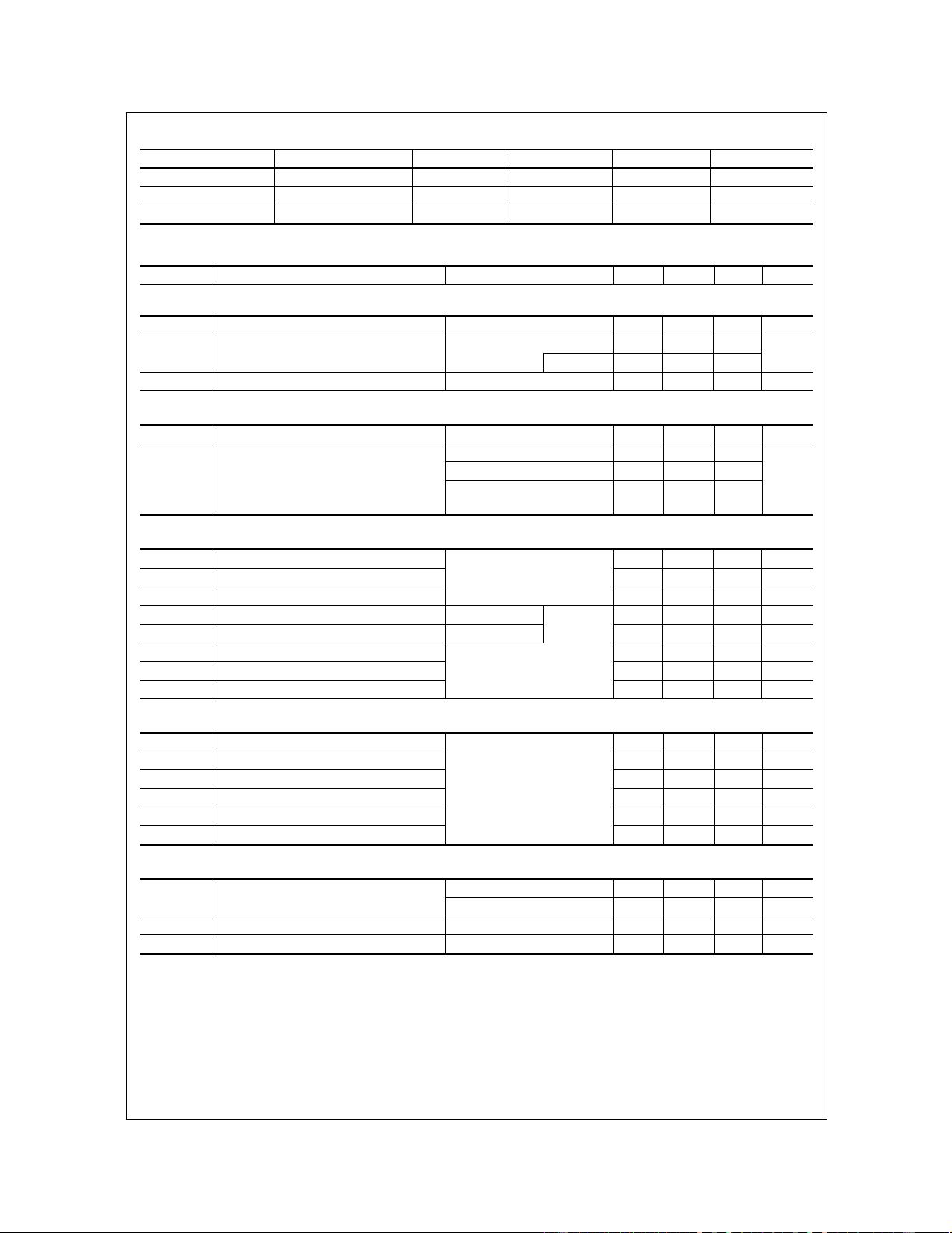
MOSFET Maximum Ratings T
C
= 25°C unless otherwise noted
Thermal Characteristics
This product has been designed to meet the extreme test conditions and environment demanded by the automotive industry. For a
copy of the requirements, see AEC Q101 at: http://www.aecouncil.com/
Reliability data can be found at: http://www.fairchildsemi.com/products/discrete/reliability/index.html.
All Fairchild Semiconductor products are manufactured, assembled and tested under ISO9000 and QS9000 quality systems
certification.
Symbol Parameter Ratings Units
V
DSS
Drain to Source Voltage 150 V
V
GS
Gate to Source Voltage ±20 V
I
D
Drain Current
79 A
Continuous (T
C
= 25
o
C, V
GS
= 10V)
Continuous (T
C
= 100
o
C, V
GS
= 10V) 56 A
Continuous (T
amb
= 25
o
C, V
GS
= 10V, R
θJA
= 43
o
C/W) 8 A
Pulsed Figure 4 A
E
AS
Single Pulse Avalanche Energy (Note 1) 400 mJ
P
D
Power dissipation 310 W
Derate above 25
o
C2.07W/
o
C
T
J
, T
STG
Operating and Storage Temperature -55 to 175
o
C
R
θJC
Thermal Resistance Junction to Case TO-220, TO-263, TO-262 0.48
o
C/W
R
θJA
Thermal Resistance Junction to Ambient TO-220, TO-262 (Note 2) 62
o
C/W
R
θJA
Thermal Resistance Junction to Ambient TO-263, 1in
2
copper pad area 43
o
C/W
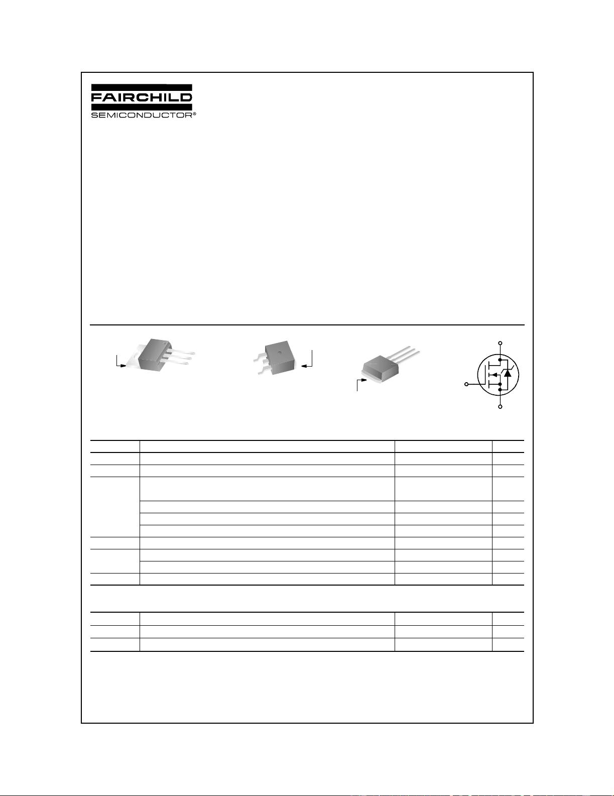
S
G
D
TO-263AB
FDB SERIES
TO-220AB
FDP SERIES
DRAIN
DRAIN
GATE
GATE
SOURCE
SOURCE
(FLANGE)
DRAIN
(FLANGE)
DRAIN
(FLANGE)
DRAIN
SOURCE
GATE
TO-262AB
FDI SERIES

剩余10页未读,继续阅读
资源评论


