HIGH
VOLTAGE
THIN
LAYER
DEVICES (RESURF DEVICES)
J.A.
Appels and
H.M.J.
Vaes
Philips Research Laboratories
Eindhoven
-
The Netherlands
ABSTRACT
The application of a somewhat unusual
diode structure opens the possibility to
make novel kinds of high voltage devices
even with very thin epitaxial or implanted
layers. In the new structures crucial
changes in the electric field distribu-
tion take place at or at
least
near the
surface
II
The acronym RESURF (REduced
XJR-
face Field) was chosen.
BASIC STRUCTURE
The basic structure consists of a
high-ohmic P-substrate with an epitaxial
N-layer oniit, which
$7
laterally boun-
ded by
a
P
diffusion
.
The diode thus
formed consists of two parts: one hori-
zontal P-N junction and a vertical
PiN
junction. Considering these parts as
one-dimensional junctions, the vertical
one has the lower breakdown voltage,
which
is
determined by the doping concen-
tration of the epitaxial layer (e.g.
370
V
for
Ne
i
6.1014).
The breakdown
voltage
of
tge
Eorizontal junction
is
con-
siderably higher due to the high-ohmic
substrate
(1150
V
for the example of
fig.
1).
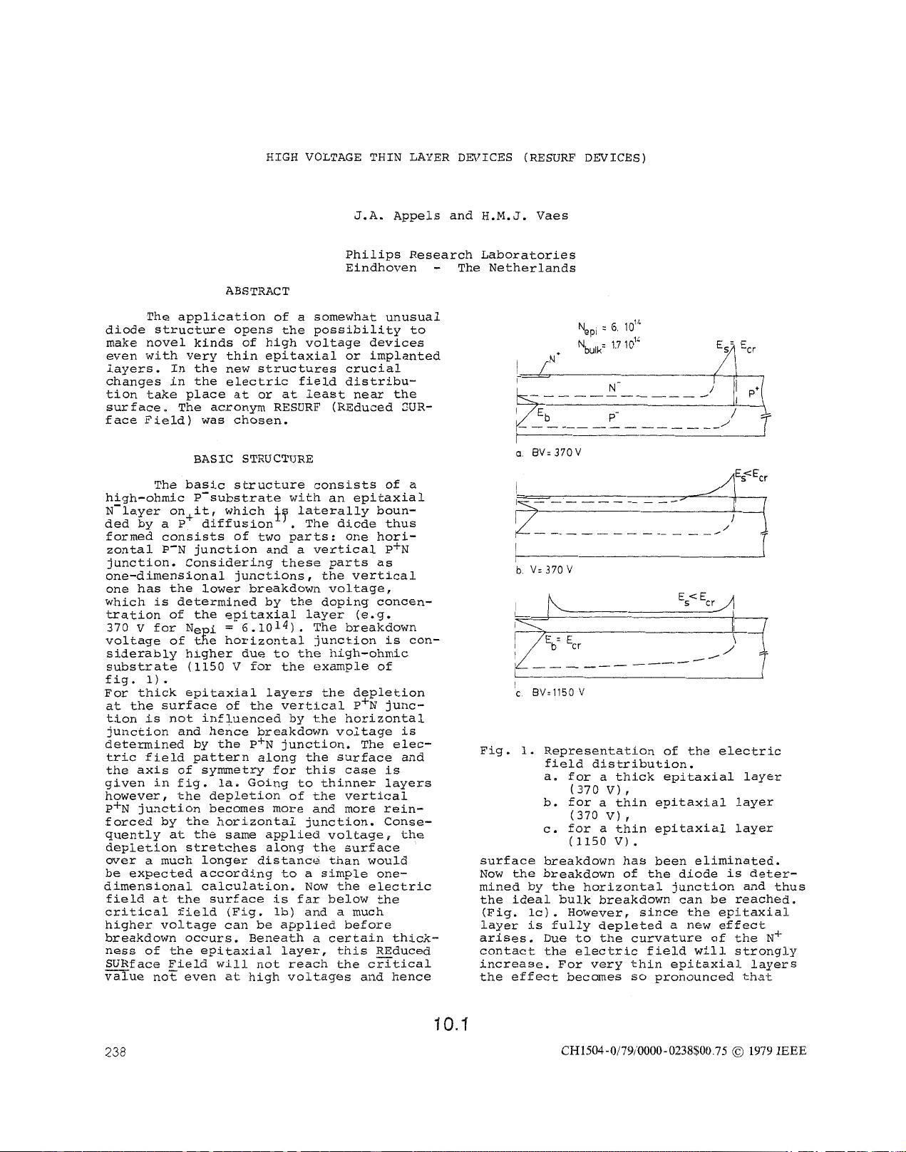
For thick epitaxial layers the depletion
at
the surface of the vertical
P'N
junc-
tion
is
not influenced by the horizontal
junction and hence breakdown voltage
is
determined by the
P'N
junction. The
elec-
tric
field pattern along the surface and
the axis of symmetry for this case
is
given in fig
.
la.
Going to thinner layers
however, the depletion of the vertical
P+N
junction becomes more and more rein-
forced by the horizontal junction. Conse-
quently
at
the
same
applied voltage, the
depletion stretches along the surface
mer
a much longer distance than would
be expected according to a simple one-
dimensional calculation. Now the
electric
field at the surface
is
far below the
critical field (Fig. lb) and a much
higher voltage can be applied before
breakdown occurs. Beneath a certain thick-
ness
of
the epitaxial layer, this gduced
SURface Field
will
not reach the critical
xue not even
at
high volt.ages and hence
a,
BV=
370V
'J
b.
V:
370V
Fig.
1.
Representation of the
electric
field distribution.
a. for a thick epitaxial layer
b. for
a
thin epitaxial layer
c.
for a thin epitaxial layer
(370
VI,
(370
V)
I
(1150
V)
.
surface breakdown has been eliminated.
Now the breakdown of the diode
is
deter-
mined by the horizontal junction and thus
the ideal bulk breakdown can be reached.
(Fig.
IC)
However, since the epitaxial
layer
is
fully depleted a new effect
arises. Due to the curvature
of
the
N'
contact the
electric
field
will
strongly
increase. For very thin epitaxial layers
the effect becomes
so
pronounced that
238
CH1504-0/79/0000-0238$00.75
0
1979
IEEE


 我的内容管理
展开
 我的资源
快来上传第一个资源
 我的收益 登录查看自己的收益
 我的积分
登录查看自己的积分
 我的C币
登录后查看C币余额
 我的收藏
我的收藏  我的下载
我的下载  下载帮助
下载帮助 
 前往需求广场,查看用户热搜

 信息提交成功