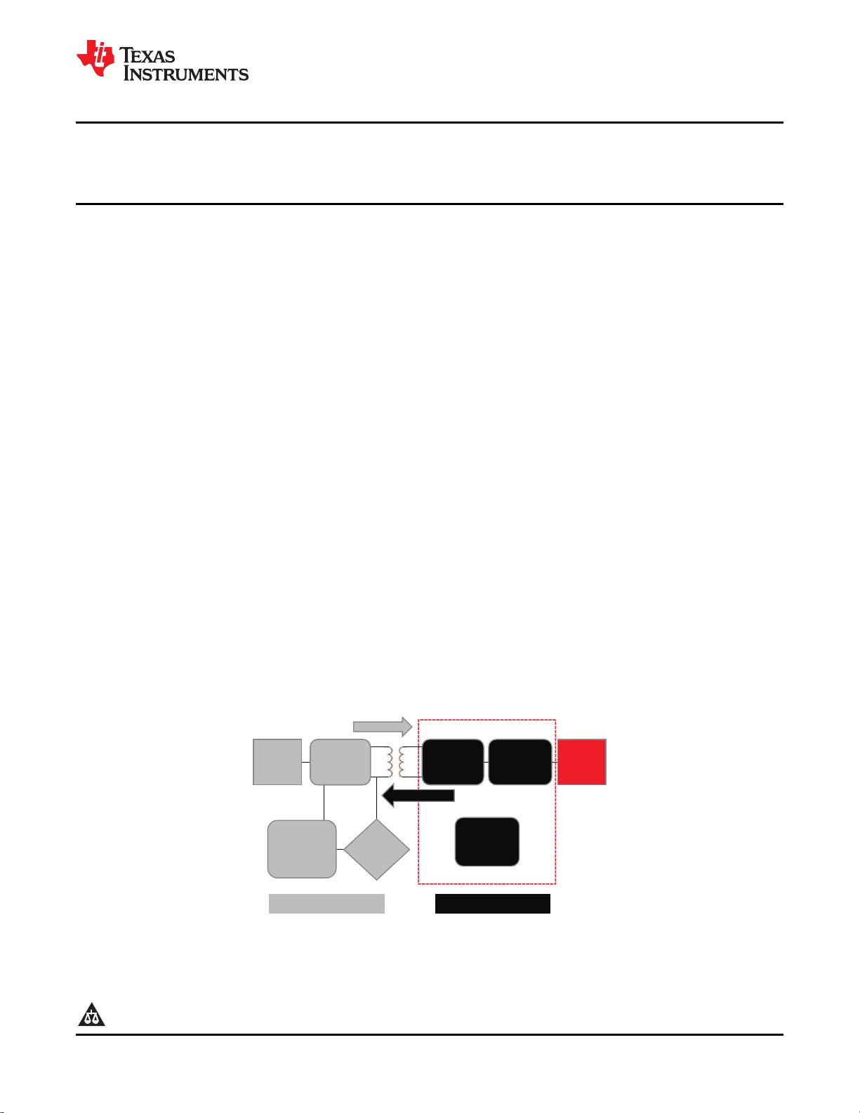
没有合适的资源?快使用搜索试试~ 我知道了~
TI 无线充电接受器,符合QI无线电源联盟标准,93%的整体峰值AC\DC效率
资源推荐
资源详情
资源评论
AC to DC
Voltage
Conditioning
Controller
RectificationDrivers RectificationDrivers Load
Controller
V/I
Sense
Power
Transmitter Receiver
bqTESLA150LP: Receiver Integration 1/5 of the Area Savings
th
bq5101x
bq500210
Communication
bq51011
bq51013
www.ti.com.cn
ZHCS113D –APRIL 2011–REVISED AUGUST 2012
集集成成型型无无线线电电源源接接收收器器,,
符符合合 Qi ((无无线线电电源源联联盟盟))标标准准
查查询询样样品品: bq51011, bq51013
1
特特性性
• 支支持持 5-V 稳稳压压电电源源的的集集成成型型无无线线电电源源接接收收器器解解决决方方 • 数数码码摄摄像像机机
案案
• 便便携携式式媒媒体体播播放放器器
– 93% 的的整整体体峰峰值值 AC-DC 效效率率
• 手手持持式式设设备备
– 完完全全同同步步整整流流器器
说说明明
– 符符合合 WPC v1.0 标标准准的的通通信信控控制制
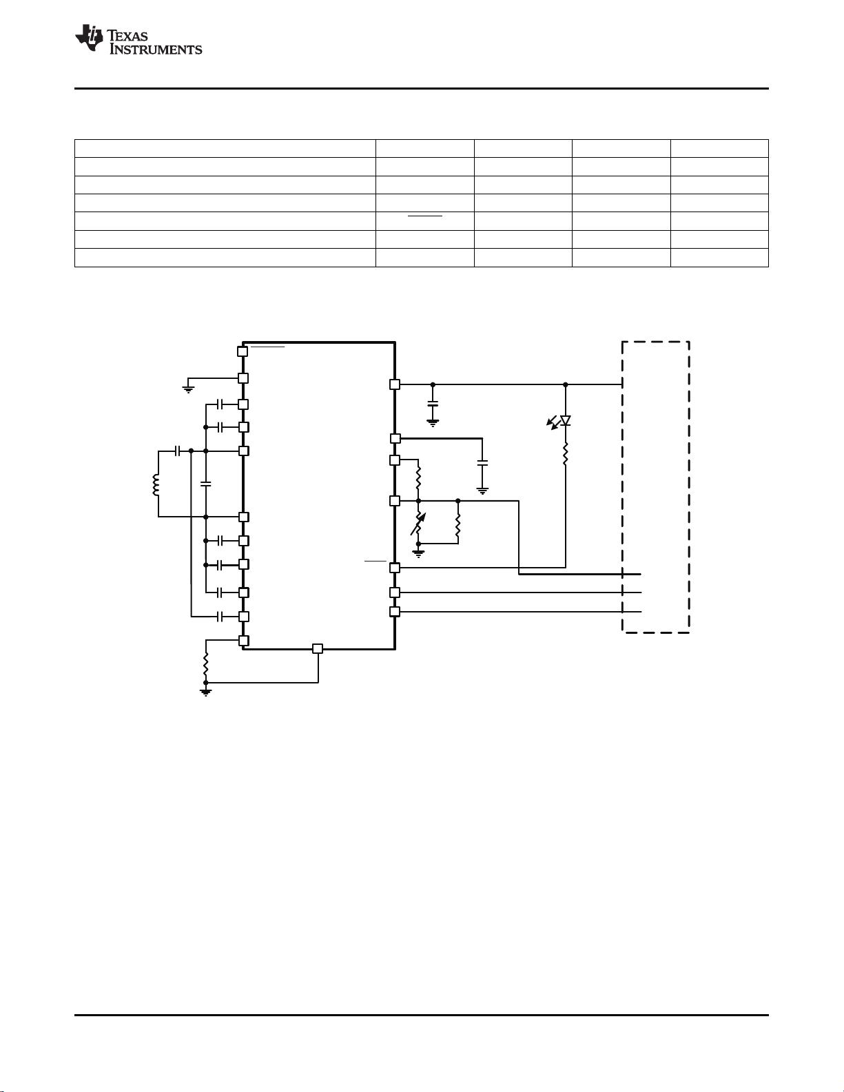
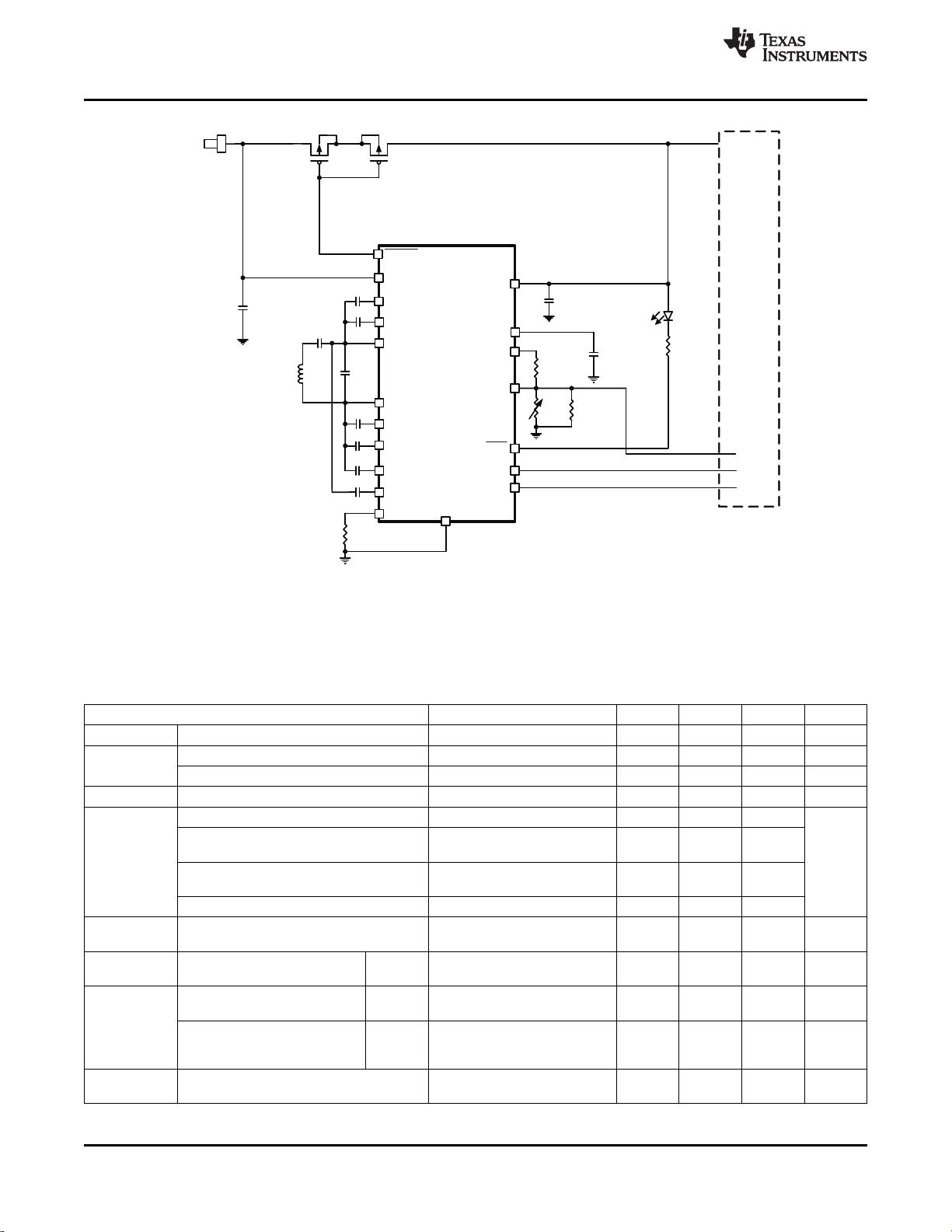
bq5101x 是一款适用于便携式应用无线电源传输的集
– 输输出出电电压压调调节节
成型高级接收器 IC, 此器件不但提供 AC/DC 电源转
– RX 线线圈圈与与 5-V DC 输输出出电电压压之之间间仅仅需需的的 IC
换,同时还集成符合 Qi v1.0 通信协议标准所需的数字
• 动动态态整整流流器器控控制制可可提提高高负负载载瞬瞬态态响响应应
控制功能。 bq5101x 与 bq500210 发送器控制器相结
• 支支持持 20-V 最最大大输输入入
合,可为无线电源解决方案实现完整的非接触式电源传
• 低低功功耗耗耗耗散散整整流流器器过过压压钳钳位位 (V
OVP
= 15 V)
输系统。 嵌入在便携式设备中的接收器线圈采用近场
• 热热关关断断
感应电源传输,可通过相互耦合的电感器接受发送器发
• 单单个个 NTC//控控制制引引脚脚可可实实现现最最佳佳安安全全性性与与主主机机间间
送的电源。 来自接收器线圈的 AC 信号此后经过整流
I/O
和调节,可用作系统关闭电子产品 (down-system
• 独独立立数数字字控控制制器器
electronics) 的电源。 全局反馈通过仅次于发送器的机
• 采采用用 1.9 x 3mm 晶晶圆圆级级芯芯片片规规模模封封装装 (DSBG) 或或
4.5 x 3.5mm 四四方方扁扁平平无无引引线线 (QFN) 封封装装
制建立,以通过反散射调制稳定电源传输过程。 该反
馈采用 Qi v1.0 通信协议建立后,可支持高达 5-W 的
应应用用范范围围
应用。
• 符符合合 WPC 标标准准的的接接收收器器
该器件集成了一个低阻抗完全同步整流器、低压降稳压
• 手手机机与与智智能能电电话话
器、数字控制、和精确电压与电流环路。 整个功率级
• 耳耳机机
(整流器与 LDO) 均采用低电阻 NMOS FET 技术确
保高效率与低功耗。
Figure 1. Wireless Power Consortium (WPC or Qi) Inductive Power System
1
Please be aware that an important notice concerning availability, standard warranty, and use in critical applications of
Texas Instruments semiconductor products and disclaimers thereto appears at the end of this data sheet.
PRODUCTION DATA information is current as of publication date.
Copyright © 2011–2012, Texas Instruments Incorporated
Products conform to specifications per the terms of the Texas
Instruments standard warranty. Production processing does not English Data Sheet: SLVSAT9
necessarily include testing of all parameters.
bq51011
bq51013
ZHCS113D –APRIL 2011–REVISED AUGUST 2012
www.ti.com.cn
These devices have limited built-in ESD protection. The leads should be shorted together or the device placed in conductive foam
during storage or handling to prevent electrostatic damage to the MOS gates.
ORDERING INFORMATION
Ordering Number
Part NO Marking Function Package Quantity
(Tape and Reel)
bq51013YFFR 3000
bq51013 DSBGA-YFF
bq51013YFFT 250
bq51013 5V Regulated Power Supply
bq51013RHLR 3000
WAES QFN-RHL
(1)
bq51013RHLT 250
bq51011YFFR 3000
bq51011 bq51011 Current Limited Power Supply DSBGA-YFF
bq51011YFFT 250
(1) Product Preview
AVAILABLE OPTIONS
Communication
Device Function V
AD_OVP
V
RECT-OVP
V
RECT(REG)
V
OUT(REG)
Current Limit
bq51013 5V Power Supply 15V Dynamic 5V None
none
5V Current Limited 400mA + Dynamic
bq51011 15V Tracks V
OUT
5V
Power Supply I
Lim
ABSOLUTE MAXIMUM RATINGS
(1)(2)
over operating free-air temperature range (unless otherwise noted)
VALUES
PARAMETER PIN UNITS
MIN MAX
AC1, AC2, RECT, COMM1, COMM2, OUT, V
-0.3 20
CHG
Input Voltage
AD, AD-EN -0.3 30 V
BOOT1, BOOT2 -0.3 26 V
Input Current AC1, AC2 1 A(RMS)
Output Current OUT 1.5 A
CHG 15 mA
Output Sink Current
COMM1, COMM2 1 A
Junction temperature, T
J
-40 150 °C
Storage temperature, T
STG
-65 150 °C
ESD Rating (HBM) (100pF, 1.5KΩ) All 2KV
(1) All voltages are with respect to the VSS terminal, unless otherwise noted.
(2) Stresses beyond those listed under absolute maximum ratings may cause permanent damage to the device. These are stress ratings
only, and functional operation of the device at these or any other conditions beyond those indicated under recommended operating
conditions is not implied. Exposure to absolute-maximum-rated conditions for extended periods may affect device reliability.
THERMAL INFORMATION
RHL YFF
THERMAL METRIC
(1)
UNITS
20 PiNS 28 PINS
θ
JA
Junction-to-ambient thermal resistance 37.7 58.9
θ
JCtop
Junction-to-case (top) thermal resistance 35.5 0.2
θ
JB
Junction-to-board thermal resistance 13.6 9.1
°C/W
ψ
JT
Junction-to-top characterization parameter 0.5 1.4
ψ
JB
Junction-to-board characterization parameter 13.5 8.9
θ
JCbot
Junction-to-case (bottom) thermal resistance 2.7 n/a
(1) For more information about traditional and new thermal metrics, see the IC Package Thermal Metrics application report, SPRA953.
2 Copyright © 2011–2012, Texas Instruments Incorporated
System
Load
bq5101x
PGND
OUT
EN1
AD
AD-EN
CHG
C4
EN2
C1
C2
C
BOOT1
C
BOOT2
AC1
AC2
COMM2
ILIM
R1
CLAMP2
C
COMM2
C
CLAMP2
COIL
BOOT1
RECT
C3
R2
NTC
VTSB
TS/CTRL
R4
D1
BOOT2
R3
CLAMP1
C
CLAMP1
C
COMM1
COMM1
HOST
3-State
Bi-State
Bi-State
bq51011
bq51013
www.ti.com.cn
ZHCS113D –APRIL 2011–REVISED AUGUST 2012
RECOMMENDED OPERATING CONDITIONS
over operating free-air temperature range (unless otherwise noted)
PARAMETER PINS MIN MAX UNITS
Input voltage range, V
IN
RECT 4 10 V
Input current, I
IN
RECT 1.5 A
Output current, I
OUT
OUT 1.5 A
Sink current, I
AD-EN
AD-EN 1 mA
COMM sink current, I
COMM
COMM 500 mA
Junction Temperature, T
J
0 125 ºC
TYPICAL APPLICATION SCHEMATICS
Figure 2. bq5101x Used as a Wireless Power Receiver and Power Supply for System Loads
Copyright © 2011–2012, Texas Instruments Incorporated 3
USB or
AC Adapter
Input
System
Load
Q1
C5
bq5101x
PGND
OUT
EN1
AD
AD-EN
CHG
C4
EN2
C1
C2
C
BOOT1
C
BOOT2
AC1
AC2
COMM2
ILIM
R1
CLAMP2
C
COMM2
C
CLAMP2
COIL
BOOT1
RECT
C3
R2
NTC
VTSB
TS/CTRL
R4
D1
BOOT2
R3
CLAMP1
C
CLAMP1
C
COMM1
COMM1
HOST
3-State
Bi-State
Bi-State
bq51011
bq51013
ZHCS113D –APRIL 2011–REVISED AUGUST 2012
www.ti.com.cn
Figure 3. bq5101x Used as a Wireless Power Receiver and Power Supply for System Loads With Adapter
Power-Path Multiplexing
ELECTRICAL CHARACTERISTICS
over operating free-air temperature range, 0°C to 125°C (unless otherwise noted)
PARAMETER TEST CONDITIONS MIN TYP MAX UNIT
UVLO Undervoltage lock-out V
RECT
: 0V → 3V 2.6 2.7 2.8 V
Hysteresis on UVLO V
RECT
: 3V → 2V 250 mV
V
HYS
Hysteresis on OVP V
RECT
: 16V → 5V 150 mV
V
RECT
Input overvoltage threshold V
RECT
: 5V → 16V 14.5 15 15.5 V
Dynamic V
RECT
Threshold 1 I
LOAD
< 100 mA (I
LOAD
rising) 7.08
100 mA < I
LOAD
< 200 mA
Dynamic V
RECT
Threshold 2 6.28
(I
LOAD
rising)
V
RECT-REG
(1)
V
200 mA < I
LOAD
< 400 mA
Dynamic V
RECT
Threshold 3 5.53
(I
LOAD
rising)
Dynamic V
RECT
Threshold 4 I
LOAD
> 400 mA (I
LOAD
rising) 5.11
I
LOAD
Hysteresis for dynamic V
RECT
I
LOAD
I
LOAD
falling 40 mA
thresholds
Tracking V
RECT
regulation V
OUT
= 3.5 V, I
OUT
= K
ILIM
/
V
RECT-TRACK
bq51011 250 mV
above V
OUT
R
ILIM
> 250mA
Percentage of I
LIM
at which
bq51011 I
LOAD
rising 60%
V
RECT(REG)
begins to track V
OUT
I
RECT-REG
Hysteresis percentage of I
LOAD
at which V
RECT(REG)
halts bq51011 I
LOAD
falling 20%
tracking VOUT
Rectifier undervoltage protection, restricts
V
RECT-DPM
3 3.1 3.2 V
I
OUT
at V
RECT-DPM
(1) For the bq51011, V
RECT-REG
only applies when V
RECT-TRACK
is not active.
4 Copyright © 2011–2012, Texas Instruments Incorporated
bq51011
bq51013
www.ti.com.cn
ZHCS113D –APRIL 2011–REVISED AUGUST 2012
ELECTRICAL CHARACTERISTICS (continued)
over operating free-air temperature range, 0°C to 125°C (unless otherwise noted)
PARAMETER TEST CONDITIONS MIN TYP MAX UNIT
Rectifier reverse voltage protection when a V
RECT-REV
= V
OUT
- V
RECT
,
V
RECT-REV
9 8 V
supply is present at V
OUT
V
OUT
= 10V
Quiescent Current
I
LOAD
= 0mA, 0°C ≤ T
J
≤ 85°C 8 10 mA
Active chip quiescent current consumption
I
RECT
I
LOAD
= 300mA, 0°C ≤ T
J
≤
from RECT
2 2.5 mA
85°C
Quiescent current at the output when
I
OUT
V
OUT
= 5V, 0°C ≤ T
J
≤ 85°C 20 35 µA
wireless power is disabled (Standby)
I
LIM
Short Circuit
Highest value of I
LIM
resistor considered a R
ILIM
: 200Ω → 50Ω. I
OUT
R
ILIM
120 Ω
fault (short). Monitored for I
OUT
> 100 mA latches off, cycle power to reset
Deglitch time transition from I
LIM
short to
t
DGL
1 ms
I
OUT
disable
I
LIM-SHORT,OK
enables the I
LIM
short
I
LIM_SC
comparator when I
OUT
is greater than this I
LOAD
: 0 → 200mA 90 105 125 mA
value
Maximum I
LOAD
that will be
I
OUT
Maximum output current limit, C
L
delivered for 1 ms when I
LIM
is 2.4 A
shorted
OUTPUT
I
LOAD
= 1000 mA 4.85 4.95 5
V
OUT-REG
Regulated output voltage V
I
LOAD
= 1 mA 4.95 5 5.05
V
DO
Drop-out voltage, RECT to OUT I
LOAD
= 1A 110 190 mV
K
ILIM
Current programming factor R
LIM
= K
ILIM
/ I
ILIM
, I
LOAD
= 1 A 280 300 320 AΩ
I
ILIM
Current limit programming range 1500 mA
OUT pin short-circuit
bq51011 V
OUT
: 3 V → 0.5 V, no deglitch 0.7 0.8 0.9 V
detection/pre-charge threshold
V
OUT_SC
V
OUT_SC
hysteresis bq51011 V
OUT
: 0.5 V → 3 V 100 mV
Current limit during WPC
I
COMM
(2)
bq51011 I
LOAD
= I
ILIM
365 390 420 mA
communication
Source current to OUT pin
I
OUT_SC
bq51011 V
OUT
= 0V, 0°C ≤ T
J
≤ 85°C 15 25 mA
during short-circuit detection
TS / CTRL
I
TS-Bias
< 100µA (periodically
V
TS
TS Bias Voltage 2.1 2.2 2.3 V
driven see t
TS
/CTRL-Meas)
I
TS
TS-Bias Short circuit protection V
TS-Bias
= 0V 1 3 mA
Rising threshold V
TS
: 50% → 60% 54 56 58
V
COLD
Falling hysteresis V
TS
: 60% → 50% 1
%V
TS-Bias
Falling threshold V
TS
: 20% → 15% 17 18 19
V
HOT
Rising hysteresis V
TS
: 15% → 20% 1
CTRL pin threshold for a high V
TS/CTRL
: 50 → 150mV 80 100 130 mV
V
CTRL
CTRL pin threshold for a low V
TS/CTRL
: 150 → 50mV 50 80 100 mV
Time VTS-Bias is active when TS Synchronous to the
t
TS/CTRL
24 ms
measurements occur communication period
t
TS
Deglitch time for all TS comparators 10 ms
THERMAL PROTECTION
Thermal shutdown temperature 155 °C
T
J
Thermal shutdown hysteresis 20 °C
(2) Dynamic communication current limit enables the 400mA current limit only when the output current is equal to the programmed current
limit (I
ILIM
) for the bq51011.
Copyright © 2011–2012, Texas Instruments Incorporated 5
剩余30页未读,继续阅读
资源评论
notflycn
- 粉丝: 0
- 资源: 14
上传资源 快速赚钱
- 我的内容管理 展开
- 我的资源 快来上传第一个资源
- 我的收益 登录查看自己的收益
- 我的积分 登录查看自己的积分
- 我的C币 登录后查看C币余额
- 我的收藏
- 我的下载
- 下载帮助
安全验证
文档复制为VIP权益,开通VIP直接复制
信息提交成功