XAPP1286 (v1.0) June 23, 2016 1
www.xilinx.com
Summary
Creating an AXI subsystem in a Xilinx FPGA allows designers to quickly and easily generate
complex systems. When designers connect their system to PCI Express (PCIe) [Ref 2], they often
use the AXI Memory Mapped to PCIe Gen2 bridge. This method may use valuable FPGA resources
in a system which only requires simple read and write operations. This application note and
accompanying source code shows designers how to create a very small PCIe to AXI bridge
which supports 1 DWORD reads and writes from the host to the FPGA Endpoint, using a fraction
of the resources of the fully featured AXI Memory Mapped to PCIe Gen2 bridge.
Reference Design
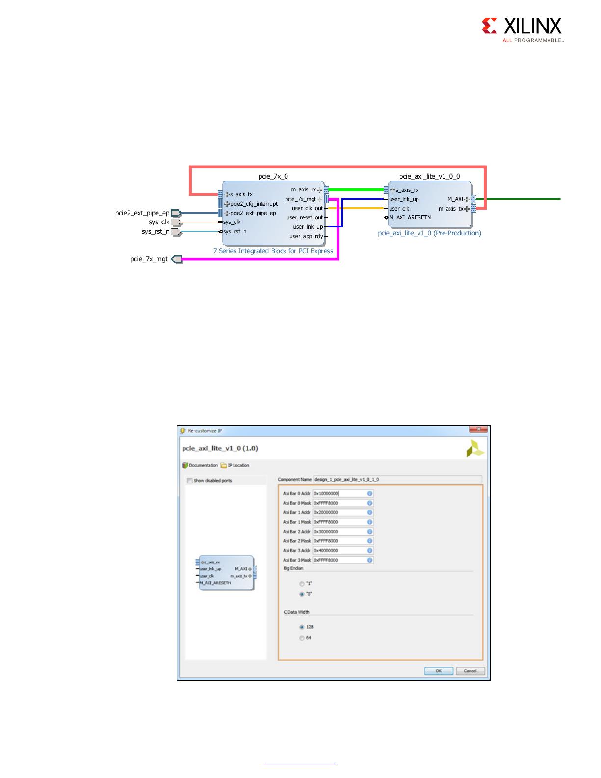
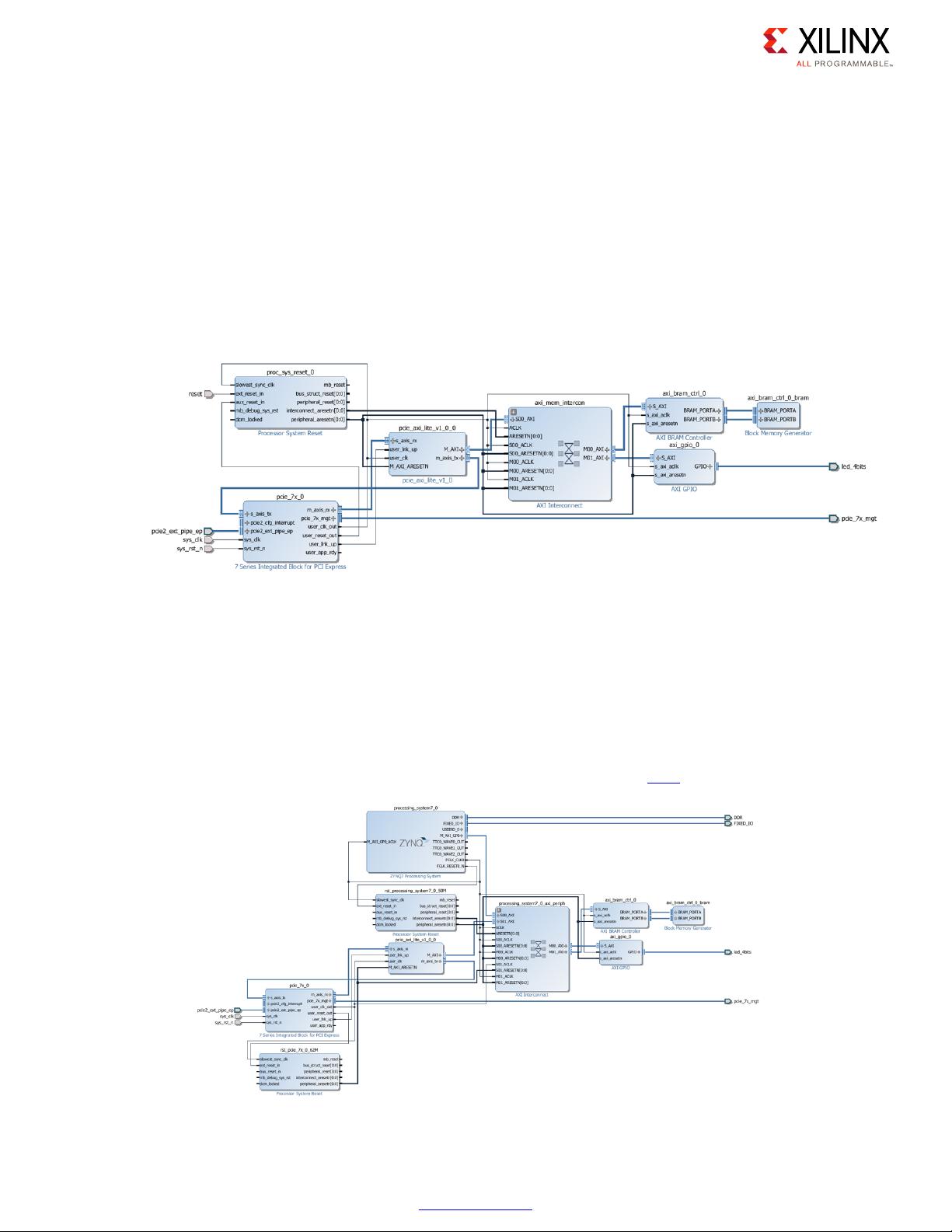
The PCIe to AXI4-Lite bridge design referenced in this application note has been packaged as a
Vivado IP core to make it easy to integrate into an IPI design. The project and source code used
to package the IP are also provided, as well as two projects which use the packaged IP targeting
the Xilinx AC701 and ZC706 Xilinx reference boards.
Feature Support
• Endpoint accepts 1 DWORD PCIe reads and writes from the Host to the FPGA Endpoint
• Connects directly to the 7 Series Integrated Block for PCIe IP core
• Supports up to four 32-bit PCIe to AXI BAR translations with address masking
• Supports Endian swapping
• Supports 64-bit and 128-bit data widths (Gen1 x1 - Gen2 x8)
Application Note: 7 Series FPGAs
XAPP1286 (v1.0) June 23, 2016
7 Series FPGAs Gen2 Integrated Block
for PCIe to AXI4-Lite Bridge
Authors: Jason Lawley, Sanjay Rai