K7A801800B
256Kx36 & 512Kx18 Synchronous SRAM
- 3 -
Rev 3.0
Nov. 2003
K7A803600B
256Kx36 & 512Kx18-bit Synchronous Pipelined Burst SRAM
The K7A803600B and K7A801800B are 9,437,184-bit Syn-
chronous Static Random Access Memory designed for high
performance second level cache of Pentium and Power PC
based System.
It is organized as 256K(512K) words of 36(18) bits and inte-
grates address and control registers, a 2-bit burst address
counter and added some new functions for high perfor-
mance cache RAM applications; GW
, BW, LBO, ZZ. Write
cycles are internally self-timed and synchronous.
Full bus-width write is done by GW
, and each byte write is
performed by the combination of WE
x and BW when GW is
high. And with CS
1 high, ADSP is blocked to control signals.
Burst cycle can be initiated with either the address status
processor(ADSP
) or address status cache controller(ADSC)
inputs. Subsequent burst addresses are generated inter-
nally in the system¢s burst sequence and are controlled by
the burst address advance(ADV
) input.
LBO
pin is DC operated and determines burst sequence(lin-
ear or interleaved).
ZZ pin controls Power Down State and reduces Stand-by
current regardless of CLK.
The K7A803600B and K7A801800B are fabricated using
SAMSUNG¢s high performance CMOS technology and is
available in a 100pin TQFP and Multiple power and ground
pins are utilized to minimize ground bounce.
GENERAL DESCRIPTIONFEATURES
• Synchronous Operation.
• 2 Stage Pipelined operation with 4 Burst.
• On-Chip Address Counter.
• Self-Timed Write Cycle.
• On-Chip Address and Control Registers.
• 3.3V+0.165V/-0.165V Power Supply.
• I/O Supply Voltage 3.3V+0.165V/-0.165V for 3.3V I/O
or 2.5V+0.4V/-0.125V for 2.5V I/O
• 5V Tolerant Inputs Except I/O Pins.
• Byte Writable Function.
• Global Write Enable Controls a full bus-width write.
• Power Down State via ZZ Signal.
• LBO
Pin allows a choice of either a interleaved burst or a linear
burst.
• Three Chip Enables for simple depth expansion with No Data
Contention only for TQFP ; 2cycle Enable, 1cycle Disable.
• Asynchronous Output Enable Control.
• ADSP
, ADSC, ADV Burst Control Pins.
• TTL-Level Three-State Output.
• 100-TQFP-1420A
• Operating in commeical and industrial temperature range.
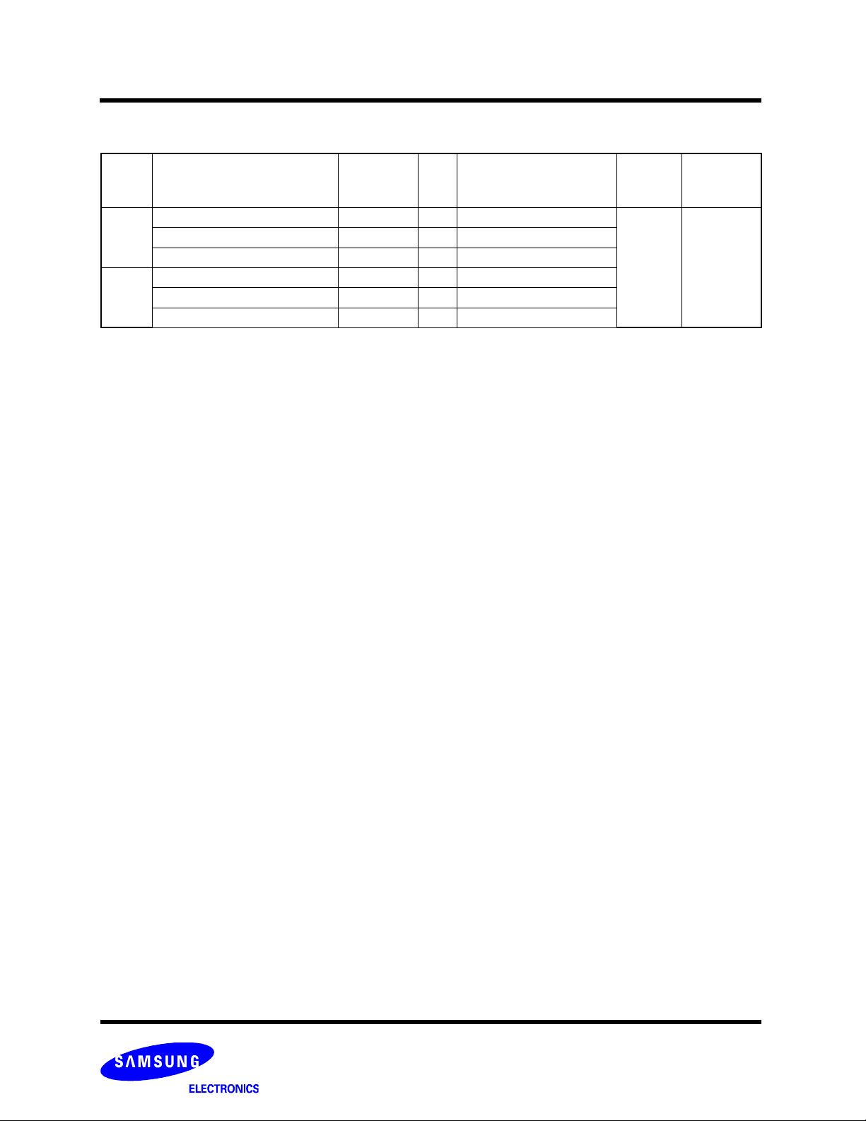
FAST ACCESS TIMES
PARAMETER Symbol -16 -14 Unit
Cycle Time tCYC 6.0 7.2 ns
Clock Access Time tCD 3.5 3.8 ns
Output Enable Access Time tOE 3.5 3.8 ns
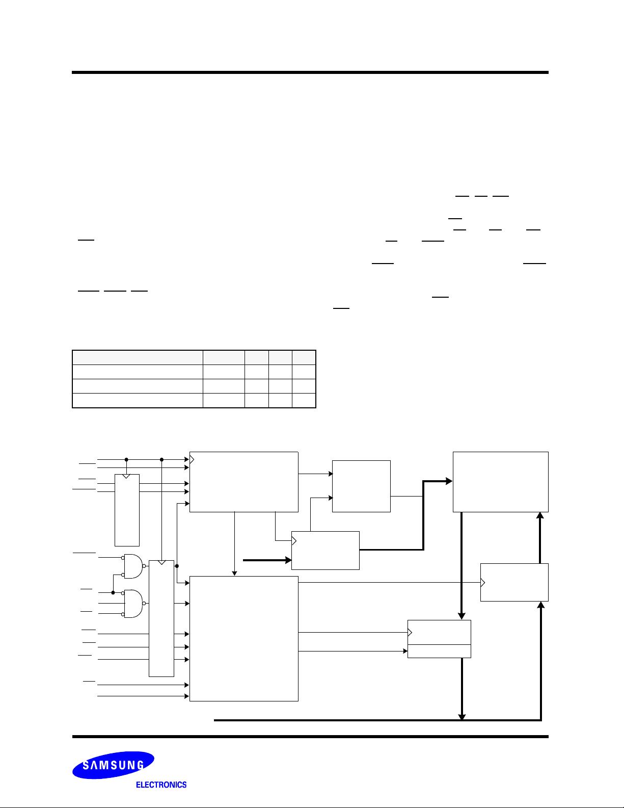
LOGIC BLOCK DIAGRAM
CLK
LBO
ADV
ADSC
ADSP
CS
1
CS
2
CS
2
GW
BW
WEx
OE
ZZ
DQa0 ~ DQd7 or DQa0 ~ DQb7
BURST CONTROL
LOGIC
BURST
256Kx36 , 512Kx18
ADDRESS
CONTROL
OUTPUT
DATA-IN
ADDRESS
COUNTER
MEMORY
ARRAY
REGISTER
REGISTER
BUFFER
LOGIC
CONTROL
REGISTER
CONTROL
REGISTER
A
′
0
~A
′
1
A
0
~A
1
or A
2
~A
18
or A
0
~A
18
REGISTER
DQPa ~ DQPd
A
0
~A
17
A
2
~A
17
(x=a,b,c,d or a,b)
DQPa,DQPb


评论0