没有合适的资源?快使用搜索试试~ 我知道了~
SC189很好用的手册
需积分: 10 3 下载量 51 浏览量
2013-06-16
23:30:46
上传
评论
收藏 1.45MB PDF 举报
温馨提示
试读
23页
SC189,很好用的手册,熟练掌握。这类芯片资源不多。大家多看看。
资源推荐
资源详情
资源评论
June 01, 2009
POWER MANAGEMENT
2.5MHz, 1.5A Synchronous
Step Down Regulator
SC189
www.semtech.com
1
Typical Application Circuit
GND
EN
C
IN
10µF
V
IN
2.9V to 5.5V
V
OUT
1.20V/1.5A
C
OUT
22µF
L
1µH
LX
VOUT
SC189C
VIN
Features
V
IN
Range: 2.9 – 5.5V
V
OUT
Options: 1.0 - 3.3V
Up to 1.5A Output Current
Ultra-Small Footprint, <1mm Height Solution
2.5MHz Switching Frequency
Eciency Up to 93%
Low Output Noise Across Load Range
Excellent Transient Response
Start Up into Pre-Bias Output
100% Duty-Cycle Low Dropout Operation
<1µA Shutdown Current
Internal Soft Start
Input Under-Voltage Lockout
Output Over-Voltage, Current Limit Protection
Over-Temperature Protection
Adjustable Output Voltage
Available in SOT23-5 package and 2mm x 2mm x
0.6mm thermally enhanced MLPD-UT6 package
-40 to +85°C Temperature Range
Fully WEEE and RoHS Compliant
Applications
Bluetooth Radios
DSC and PMPs
GPS Devices
xDSL Systems
POL Regulators
Portable HDD
Wireless LAN
Description
The SC189 is a high eciency, synchronous step-down
regulator providing up to 1.5A output current in either
an ultra-small 2mm x 2mm, low prole package or a low
cost SOT23-5 package. The device requires only three
external lter components for a complete step down
regulator solution. The input voltage range is 2.9 to 5.5V
with either factory programmed outputs from 1.0 to 3.3V
or adjustable output via an external resistor divider.
The converter operates at xed 2.5MHz switching
frequency allowing small L/C ltering components.
The voltage mode architecture is compatible with chip
inductors and capacitors for minimum PCB footprint and
lowest overall system cost. Total footprint of 25mm
2
can
be achieved - making the SC189 the ideal solution for
high density systems. Solution height of <1mm is also
possible.
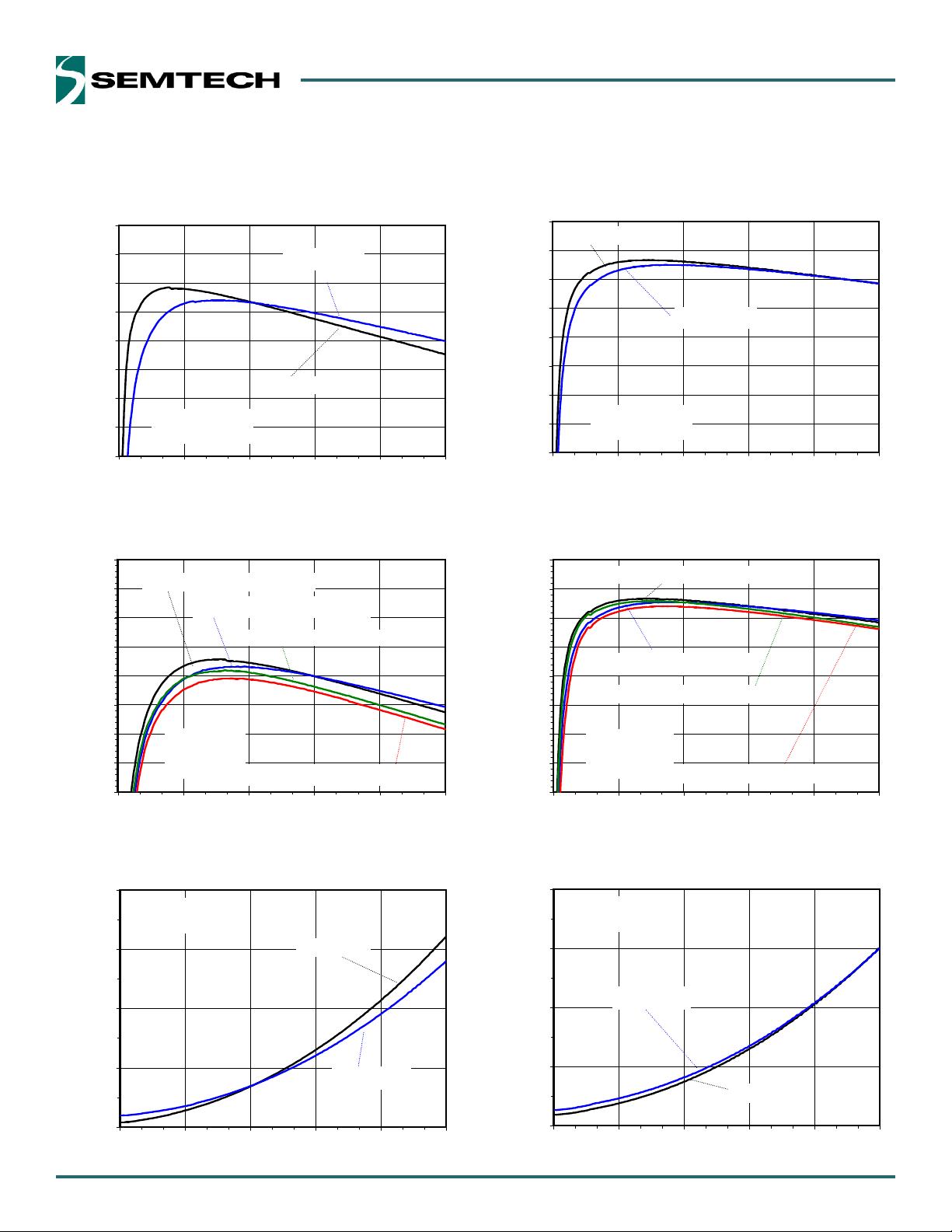
Up to 93% eciency is achieved with low R
DS(ON)
internal
switches. PWM constant frequency operation ensures
low output ripple across the load range. 100% duty-cycle
provides 360mV dropout voltage at 1.5A which extends
the minimum input voltage for 2.5V and 3.3V outputs.
Excellent transient response is achieved with no external
compensation components.
The SC189 provides input under-voltage, output over-
voltage, output short circuit and over-temperature
protection to safeguard the device and system under fault
conditions. The regulator provides integrated soft-start to
minimize inrush currents. Standby quiescient current is
less than 1µA.
The SC189 is available in SOT23-5 and a thermally
enhanced 2mm x 2mm x 0.6mm MLPD-UT6 package
rated from -40 to +85°C.
SC189
L
Chip
C
IN
0603
C
OUT
0805
Total PCB Area ~25mm
2
Actual Size
www.semtech.com© 2009 Semtech Corp.
2
SC189
Pin Conguration
Ordering Information
Marking Information
Device Package & Description
SC189xULTRT
(2)(3)(4)
2mm x 2mm x 0.6mm MLPD-UT6
SC189xSKTRT
2)(3)(4)
SOT23-5
SC189xEVB
(5)
Evaluation Board for MLPD-UT6
- Standard Size
(i.e., Wire Wound Inductor)
SC189xEVB-1
(5)
Evaluation Board for MLPD-UT6
- Small Size
(i.e., Chip Inductor)
SC189xEVB-2
(5)
Evaluation Board for SOT23-5
- Standard Size
(i.e., Wire Wound Inductor)
SC189xEVB-3
(5)
Evaluation Board for SOT23-5
- Small Size
(i.e., Chip Inductor)
Notes:
(1) Measured in free convection, mounted on 10mm x 10mm, 2 layer
FR4 PCB shown in gure 7 ( for MLPD-UT6 package) and gure 8 (
for SOT23-5 package) with copper of 1oz for each layer.
(2) Available in tape and reel only. A reel contains 3,000 devices.
(3) Available in lead-free package only. Device is WEEE and RoHS
compliant.
(4) “x” is the code of the output voltage. See Table 1 for the code. For
example, the device number for VOUT= 1.20V is SC189CULTRT.
(5) “x” is the code of the output voltage. See Table 1 for the code.
For example, the EVB for MLPD-UT6 package with VOUT= 1.20V is
SC189CEVB (Standard Size) or SC189CEVB-1 (Small Size).
Table 1: Available Output Voltages
Code
for MLPD-UT6
Code
for SOT23-5
VOUT
(1)
A A 1.00
B B 1.10
C C 1.20
E
Not Available
1.28
F
Not Available
1.30
H H 1.50
L L 1.80
N
Not Available
2.00
T Y 2.50
Not Available
V 2.70
Z Z 3.30
Notes:
(1) Contact factory for unavaliable output voltage options.
2mm x 2mm x 0.6mm MLPD-UT6
θ
JA
= 60°C/W
(1)
TOP VIEW
NC
1
2
3
6
5
4
EN
VIN
VOUT
GND
LX
T
Marking for 2mm x 2mm MLPD-UT 6 Lead Package:
x = Code of the output voltage (Example: C for VOUT=1.20V)
oyw = Pin 1 and Datecode (Reference Package Marking Design
Guidelines, Appendix A)
FLx
1
2
3
5
4
VIN
GND
EN
LX
VOUT
TOP VIEW
SOT23-5
θ
JA
= 90°C/W
(1)
189
x
Top Mark Bottom Mark
Marking for SOT23, 5 Lead Package:
x = Code of the output voltage (Example: C for VOUT=1.20V)
yyww = Datecode (Example: 0852)
www.semtech.com
© 2009 Semtech Corp.
3
SC189
Exceeding the absolute maximum ratings may result in permanent damage to the device and/or device malfunction. Operation outside of the
parameters specied in the Electrical Characteristics section is not recommended.
NOTES:
(1) Measured in free convection, mounted on 10mm x 10mm, 2 layer FR4 PCB shown in gure 7 ( for MLPD-UT6 package) and gure 8 ( for SOT23-
5 package) with copper of 1oz for each layer.
(2) Tested according to JEDEC standard JESD22-A114-B.
(3) For SOT23-5 package, the limit of the maximum power dissiption shown in gure 2 may reduce the maximum output current.
Electrical Characteristics
Recommended Operating Conditions
VIN Supply Voltage ……………………………… 2.9 to 5.5V
Maximum Output Current
(3)
…………………………… 1.5A
Temperature Range …………………………… -40 to +85˚C
Thermal Resistance, Junction to Ambient
(1)
MLPD-UT6 Package ……………………………… 60°C/W
SOT23-5 Package ……………………………… 90°C/W
Maximum Junction Temperature …………………… +150°C
Storage Temperature Range ………………… -65 to +150 °C
Thermal Information
Absolute Maximum Ratings
VIN Supply Voltage ……………………………… -0.3 to 6.0V
LX Voltage ………….. -1 to V
IN
+1V, -3V (20ns Max), 6V Max
VOUT Voltage ……………………………… -0.3 to V
IN
+0.3V
EN Voltage …………………………………. -0.3 to V
IN
+0.3V
Peak IR Reflow temperature …………………………. 260°C
ESD Protection Level
(2)
…………………………………. 3kV
Unless specied: V
IN
= 5.0V, C
IN
=10µF, C
OUT
=10µF; L=2.2µH; -40°C<T
A
<+85 °C; T
J(MAX)
=125°C; Unless otherwise noted typical values are T
A
=+25 °C.
Parameter Symbol Conditions Min Typ Max Units
Under-Voltage Lockout UVLO
Rising V
IN
2.60 2.70 2.80 V
Hysteresis 250 mV
Output Voltage Tolerance
(1)
ΔV
OUT
V
IN
=3.6V to 5.0V; No Load -2.5 +2.5 %
Current Limit I
LIMIT
Peak inductor current 2.0 A
VIN Supply Current I
Q
EN= VIN, No Load 7.5 mA
VIN Shutdown Current I
SHDN
EN= GND 1 10 µA
High Side Switch Resistance R
DSON_P
I
LX
= 100mA, for MLPD-UT6 0.13
Ω
I
LX
= -100mA, for SOT23-5 0.15
Low Side Switch Resistance R
DSON_N
I
LX
= -100mA, for MLPD-UT6 0.10
I
LX
= -100mA, for SOT23-5 0.125
LX Leakage Current I
LK(LX)
V
IN
=5.5V; L
X
=0V; EN=GND 1 10
µA
V
IN
=5.5V; L
X
=5.0V; EN=GND -10 -1
Line Regulation ΔV
LINE-REG
V
IN
= 3.6 – 5.0V; I
OUT
=0A ±1.0 %
Load Regulation
(2)
ΔV
LOAD-REG
V
IN
= 5.0V; I
OUT
=10mA – 1.5A ±1.0 %
Oscillator Frequency F
OSC
2.0 2.5 3.0 MHz
Soft-Start Time
(2)
T
SS
100 µs
EN Input High Current I
EN_HI
EN=VIN -2.0 2.0 µA
www.semtech.com© 2009 Semtech Corp.
4
SC189
Electrical Characteristics (continued)
Parameter Symbol Conditions Min Typ Max Units
EN Input Low Current I
EN_LO
EN=GND -2.0 2.0 µA
EN Input High Threshold V
EN_HI
1.2 V
EN Input Low Threshold V
EN_LO
0.4 V
VOUT Over Voltage Protection
(2)
V
OVP
115 %
Thermal Shutdown Temperature
(2)
T
SD
Junction Temperature +160 °C
Thermal Shutdown Hysteresis
(2)
T
SD_HYS
Junction Temperature 10 °C
Notes:
(1) The “Output Voltage Tolerance” includes output voltage accuracy, voltage drift over temperature and the line regulation.
(2) Guaranteed by design.
Unless specied: V
IN
= 5.0V, C
IN
=10µF, C
OUT
=10µF; L=2.2µH; -40°C<T
A
<+85 °C; T
J(MAX)
=125°C; Unless otherwise noted typical values are T
A
=+25 °C.
www.semtech.com
© 2009 Semtech Corp.
5
SC189
Typical Characteristics
Eciency vs. Load Current (V
OUT
=1.5V)
Total Loss vs. Load Current (V
OUT
=1.5V)
Losses
0
200
400
600
800
0.0 0.3 0.6 0.9 1.2 1.5
Output Current (A)
Loss (mW)
V
OUT
= 1.50V
T
A
=25°C
V
IN
= 5.0V
V
IN
= 3.3V
Losses
0
200
400
600
800
0.0 0.3 0.6 0.9 1.2 1.5
Output Current (A)
Loss (mW)
V
OUT
= 3.30V
T
A
=25°C
V
IN
= 5.0V
V
IN
= 4.0V
Eciency vs. Load Current (V
OUT
=3.3V)
Total Loss vs. Load Current (V
OUT
=3.3V)
Eciency vs. Load Current (V
IN
=5.0V, V
OUT
=1.0V)
Eciency vs. Load Current (V
IN
=5.0V, V
OUT
=3.3V)
Efficiency
60%
65%
70%
75%
80%
85%
90%
95%
100%
0.0 0.3 0.6 0.9 1.2 1.5
Output Current (A)
Efficiency (%)
L=1071AS-1R0N (33m_typ)
V
IN
= 5.0V
V
OUT
= 1.0V
T
A
=25°C
L=1071AS-2R2N (50m_typ)
L=LQM2HPN1R0MG0 (55m_typ)
L=MDT2520-CR1R0M (60m_typ)
Efficiency
60%
65%
70%
75%
80%
85%
90%
95%
100%
0.0 0.3 0.6 0.9 1.2 1.5
Output Current (A)
Efficiency (%)
V
IN
= 5.0V
V
OUT
= 3.3V
T
A
=25°C
L=1071AS-1R0N (33m_typ)
L=1071AS-2R2N (50m_typ)
L=LQM2HP1R0MG0 (55m_typ)
L=MDT2520-CR1R0M (60m_typ)
Efficiency
60%
65%
70%
75%
80%
85%
90%
95%
100%
0.0 0.3 0.6 0.9 1.2 1.5
Output Current (A)
Efficiency (%)
V
OUT
= 1.50V
T
A
=25°C
V
IN
= 5.0V
V
IN
= 3.3V
Efficiency
60%
65%
70%
75%
80%
85%
90%
95%
100%
0.0 0.3 0.6 0.9 1.2 1.5
Output Current (A)
Efficiency (%)
V
OUT
= 3.30V
T
A
=25°C
V
IN
= 5.0V
V
IN
= 4.0V
Circuit Conditions: C
IN
= 10uF/6.3V; C
OUT
= 10uF/6.3V for L=2.2uH; C
OUT
= 22uF/6.3V for L=1uH.
Unless otherwise noted, L= 2.2uH (TOKO: 1071AS-2R2M) and SC189 in MLPD-UT6 package.
剩余22页未读,继续阅读
资源评论
wukq1001
- 粉丝: 0
- 资源: 1
上传资源 快速赚钱
- 我的内容管理 展开
- 我的资源 快来上传第一个资源
- 我的收益 登录查看自己的收益
- 我的积分 登录查看自己的积分
- 我的C币 登录后查看C币余额
- 我的收藏
- 我的下载
- 下载帮助
安全验证
文档复制为VIP权益,开通VIP直接复制
信息提交成功