DS1337Serial Real-Time Clock
需积分: 3 95 浏览量
2009-08-12
17:01:35
上传
评论 1
收藏 364KB PDF 举报

1 of 13
REV: 012003
Note: Some revisions of this device may incorporate deviations from published specifications known as errata. Multiple revisions of any device
may be simultaneously available through various sales channels. For information about device errata, click here: www.maxim-ic.com/errata
.
GENERAL DESCRIPTION
The DS1337 serial real-time clock is a low-power
clock/calendar with two programmable time-of-day
alarms and a programmable square-wave output.
Address and data are transferred serially via a 2-wire,
bidirectional bus. The clock/calendar provides
seconds, minutes, hours, day, date, month, and year
information. The date at the end of the month is
automatically adjusted for months with fewer than 31
days, including corrections for leap year. The clock
operates in either the 24-hour or 12-hour format with
AM/PM indicator.
APPLICATIONS
Handhelds (GPS, POS Terminal, MP3 Player)
Consumer Electronics (Set-Top Box, VCR/Digital
Recording)
Office Equipment (Fax/Printer, Copier)
Medical (Glucometer, Medicine Dispenser)
Telecommunications (Router, Switcher, Server)
Other (Utility Meter, Vending Machine, Thermostat,
Modem)
FEATURES
§ Real-Time Clock (RTC) Counts Seconds,
Minutes, Hours, Day, Date, Month, and Year
with Leap-Year Compensation Valid Up to 2100
§ Two-Wire Serial Interface
§ Two Time-of-Day Alarms
§ Oscillator Stop Flag
§ Programmable Square-Wave Output
– Defaults to 32kHz on Power-Up
§ Available in 8-Pin DIP, SO, or mSOP
ORDERING INFORMATION
PART TEMP RANGE PIN-PACKAGE
TOP
MARK
DS1337 -40°C to +85°C 8 DIP (300mil) DS1337
DS1337S -40°C to +85°C 8 SO (150mil) DS1337
DS1337U -40°C to +85°C
8 mSOP
1337
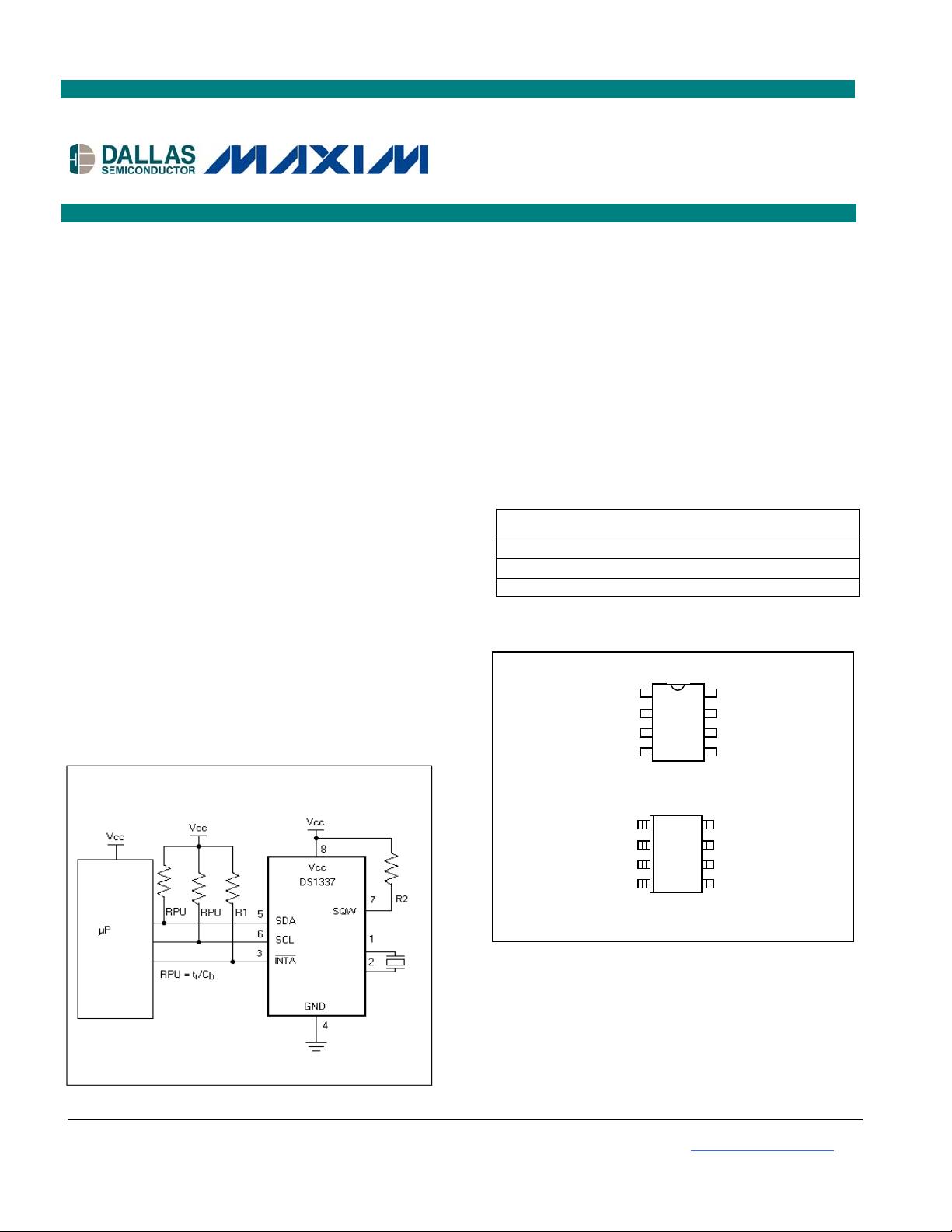
PIN CONFIGURATIONS
DS1337
Serial Real-Time Clock
www.maxim-ic.com
www.maxim-ic.com
TYPICAL OPERATING CIRCUIT
DIP
X1
X2
GND
VCC
SCL
SDA
SQW/INT
B
INTA
SO
,
m
SOP
X1
X2
GND
VCC
SCL
SDA
SQW
/
INTB
INT
A
TOP VIEW
DS1337
DS1337


剩余12页未读,继续阅读


评论0