Not
4-85
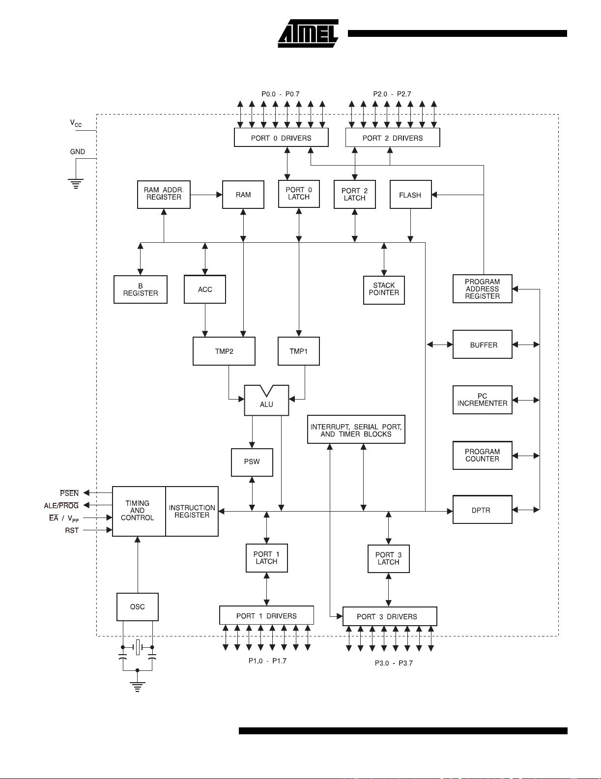
The AT89LV52 provides the following standard features:
8K bytes of Flash, 256 bytes of RAM, 32 I/O lines, three 16-
bit timer/counters, a six-vector two-level interrupt architec-
ture, a full duplex serial port, on-chip oscillator, and clock
circuitry. In addition, the AT89LV52 is designed with static
logic for operation down to zero frequency and supports
two software selectable power saving modes. The Idle
Mode stops the CPU while allowing the RAM,
timer/counters, serial port, and interrupt system to continue
functioning. The Power Down Mode saves the RAM con-
tents but freezes the oscillator, disabling all other chip func-
tions until the next hardware reset.
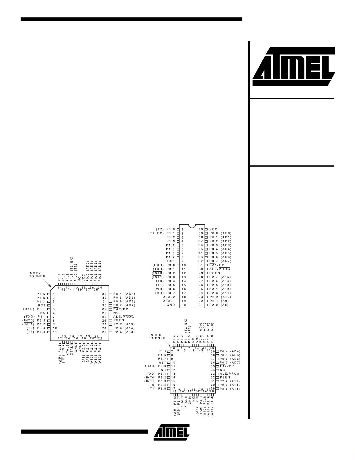
Pin Description
V
CC
Supply voltage.
GND
Ground.
Port 0
Port 0 is an 8-bit open drain bidirectional I/O port. As an
output port, each pin can sink eight TTL inputs. When 1s
are written to port 0 pins, the pins can be used as high-
impedance inputs.
Port 0 can also be configured to be the multiplexed low-
order address/data bus during accesses to external pro-
gram and data memory. In this mode, P0 has internal pul-
lups.
Port 0 also receives the code bytes during Flash program-
ming and outputs the code bytes during program verifica-
tion. External pullups are required during program verifica-
tion.
Port 1
Port 1 is an 8-bit bidirectional I/O port with internal pullups.
The Port 1 output buffers can sink/source four TTL inputs.
When 1s are written to Port 1 pins, they are pulled high by
the internal pullups and can be used as inputs. As inputs,
Port 1 pins that are externally being pulled low will source
current (I
IL
) because of the internal pullups.
In addition, P1.0 and P1.1 can be configured to be the
timer/counter 2 external count input (P1.0/T2) and the
timer/counter 2 trigger input (P1.1/T2EX), respectively, as
shown in the following table.
Port 1 also receives the low-order address bytes during
Flash programming and verification.
Port 2
Port 2 is an 8-bit bidirectional I/O port with internal pullups.
The Port 2 output buffers can sink/source four TTL inputs.
When 1s are written to Port 2 pins, they are pulled high by
the internal pullups and can be used as inputs. As inputs,
Port 2 pins that are externally being pulled low will source
current (I
IL
) because of the internal pullups.
Port 2 emits the high-order address byte during fetches
from external program memory and during accesses to
external data memory that use 16-bit addresses (MOVX @
DPTR). In this application, Port 2 uses strong internal pul-
lups when emitting 1s. During accesses to external data
memory that use 8-bit addresses (MOVX @ RI), Port 2
emits the contents of the P2 Special Function Register.
Port 2 also receives the high-order address bits and some
control signals during Flash programming and verification.
Port 3
Port 3 is an 8-bit bidirectional I/O port with internal pullups.
The Port 3 output buffers can sink/source four TTL inputs.
When 1s are written to Port 3 pins, they are pulled high by
the internal pullups and can be used as inputs. As inputs,
Port 3 pins that are externally being pulled low will source
current (I
IL
) because of the pullups.
Port 3 also serves the functions of various special features
of the AT89LV51, as shown in the following table.
Port 3 also receives some control signals for Flash pro-
gramming and verification.
RST
Reset input. A high on this pin for two machine cycles while
the oscillator is running resets the device.
ALE/PROG
Address Latch Enable is an output pulse for latching the
low byte of the address during accesses to external mem-
ory. This pin is also the program pulse input (PROG
) during
Flash programming.
In normal operation, ALE is emitted at a constant rate of 1/6
the oscillator frequency and may be used for external tim-
ing or clocking purposes. Note, however, that one ALE
Port Pin Alternate Functions
P1.0 T2 (external count input to
Timer/Counter 2), clock-out
P1.1 T2EX (Timer/Counter 2 capture/reload
trigger and direction control)
Port Pin Alternate Functions
P3.0 RXD (serial input port)
P3.1 TXD (serial output port)
P3.2 INT0
(external interrupt 0)
P3.3 INT1
(external interrupt 1)
P3.4 T0 (timer 0 external input)
P3.5 T1 (timer 1 external input)
P3.6 WR
(external data memory write strobe)
P3.7 RD
(external data memory read strobe)


 我的内容管理
展开
 我的资源
快来上传第一个资源
 我的收益 登录查看自己的收益
 我的积分
登录查看自己的积分
 我的C币
登录后查看C币余额
 我的收藏
我的收藏  我的下载
我的下载  下载帮助
下载帮助 
 前往需求广场,查看用户热搜

 信息提交成功