没有合适的资源?快使用搜索试试~ 我知道了~
TLS820F0EL V50 英飞凌芯片 INFINEON 中文版规格书手册.pdf
需积分: 5 0 下载量 139 浏览量
2023-07-10
09:18:09
上传
评论
收藏 1.3MB PDF 举报
温馨提示
![preview](https://dl-preview.csdnimg.cn/88026931/0001-960790bc32f189fbd0396a3da370690c_thumbnail.jpeg)
![preview-icon](https://csdnimg.cn/release/downloadcmsfe/public/img/scale.ab9e0183.png)
试读
40页
TLS820F0EL V50 英飞凌芯片 INFINEON 中文版规格书手册
资源推荐
资源详情
资源评论
![](https://csdnimg.cn/release/download_crawler_static/88026931/bg1.jpg)
Datasheet Rev. 1.2
www.infineon.com/OPTIREG-linear 1 2021-04-08
OPTIREG™ linear TLS820F0ELVxx
Low dropout linear voltage regulator
Features
• Wide input voltage range from 3.0 V to 40 V
• Fixed output voltage 5 V or 3.3 V
• Output voltage precision ≤ ±2 %
• Output current capability up to 200 mA
• Ultra low current consumption typ. 40 µA
• Very low dropout voltage typ. 70 mV @100 mA
• Stable with ceramic output capacitor of 1 µF
• Delayed reset at power-on with 2 Programmable delay times 8.5 ms / 16.5 ms
• Adjustable reset threshold down to 2.50 V
• Watchdog with flexible timings and current dependent deactivation: 16 ms / 32 ms / 48 ms / 96 ms,
Activated at I
Q
>5.5mA
• Enable, undervoltage reset, overtemperature shutdown
• Output current limitation
• Wide temperature range
• Green product (RoHS compliant)
Potential applications
• Automotive general ECUs
• Dashboard and cluster supplies
• Powertrain and EPS applications
• Microcontroller supply for safety applications
Product validation
Qualified for automotive applications. Product validation according to AEC-Q100/101.
Description
The OPTIREG™ linear TLS820F0ELVxx is a high performance very low dropout linear voltage regulator for 5 V
(TLS820F0ELV50) or 3.3 V (TLS820F0ELV33) supply in a PG-SSOP-14 package.
With an input voltage range of 3 V to 40 V and very low quiescent of only 40 µA, these regulators are perfectly
suitable for automotive or any other supply systems connected to the battery permanently. The TLS820F0
provides an output voltage accuracy of 2 % and a maximum output current up to 200 mA.
![](https://csdnimg.cn/release/download_crawler_static/88026931/bg2.jpg)
Datasheet 2 Rev. 1.2
2021-04-08
OPTIREG™ linear TLS820F0ELVxx
Low dropout linear voltage regulator
The new loop concept combines fast regulation and very good stability while requiring only one small ceramic
capacitor of 1 µF at the output. At currents below 100 mA the device will have a very low typical dropout
voltage of only 70 mV (for 5 V device) and 80 mV (for 3.3 V device). The operating range starts already at input
voltages of only 3 V (extended operating range). This makes the TLS820F0 also suitable to supply automotive
systems that need to operate during cranking condition.
The device can be switched on and off by the enable feature as described in Chapter 4.5.
The output voltage is supervised by the reset feature, including undervoltage reset, delayed reset at power-on
and an adjustable lower reset threshold. More details can be found in Chapter 4.7.
In addition, a watchdog circuit with flexible timings is integrated to monitor the microcontroller‘s operation.
Internal protection features like output current limitation and overtemperature shutdown are implemented
to protect the device against immediate damage due to failures like output short circuit to GND, over-current
and over-temperatures.
External components
An input capacitor C
I
is recommended to compensate line influences. The output capacitor C
Q
is necessary for
the stability of the regulating circuit. TLS820F0 is designed to be also stable with low ESR ceramic capacitors.
Type Package Marking
TLS820F0ELV50 PG-SSOP-14 820F0V50
TLS820F0ELV33 PG-SSOP-14 820F0V33
![](https://csdnimg.cn/release/download_crawler_static/88026931/bg3.jpg)
Datasheet 3 Rev. 1.2
2021-04-08
OPTIREG™ linear TLS820F0ELVxx
Low dropout linear voltage regulator
Features . . . . . . . . . . . . . . . . . . . . . . . . . . . . . . . . . . . . . . . . . . . . . . . . . . . . . . . . . . . . . . . . . . . . . . . . 1
Potential applications . . . . . . . . . . . . . . . . . . . . . . . . . . . . . . . . . . . . . . . . . . . . . . . . . . . . . . . . . . . . . 1
Product validation . . . . . . . . . . . . . . . . . . . . . . . . . . . . . . . . . . . . . . . . . . . . . . . . . . . . . . . . . . . . . . . . 1
Description . . . . . . . . . . . . . . . . . . . . . . . . . . . . . . . . . . . . . . . . . . . . . . . . . . . . . . . . . . . . . . . . . . . . . . 1
Table of contents . . . . . . . . . . . . . . . . . . . . . . . . . . . . . . . . . . . . . . . . . . . . . . . . . . . . . . . . . . . . . . . . . 3
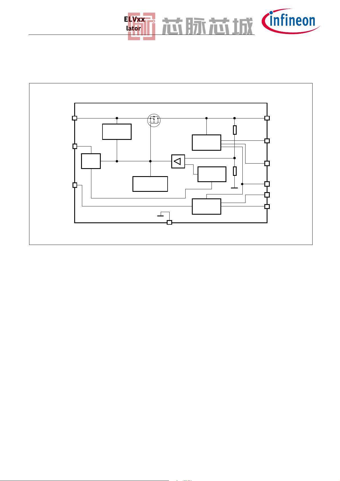
1 Block diagram . . . . . . . . . . . . . . . . . . . . . . . . . . . . . . . . . . . . . . . . . . . . . . . . . . . . . . . . . . . . . . . . . . . 4
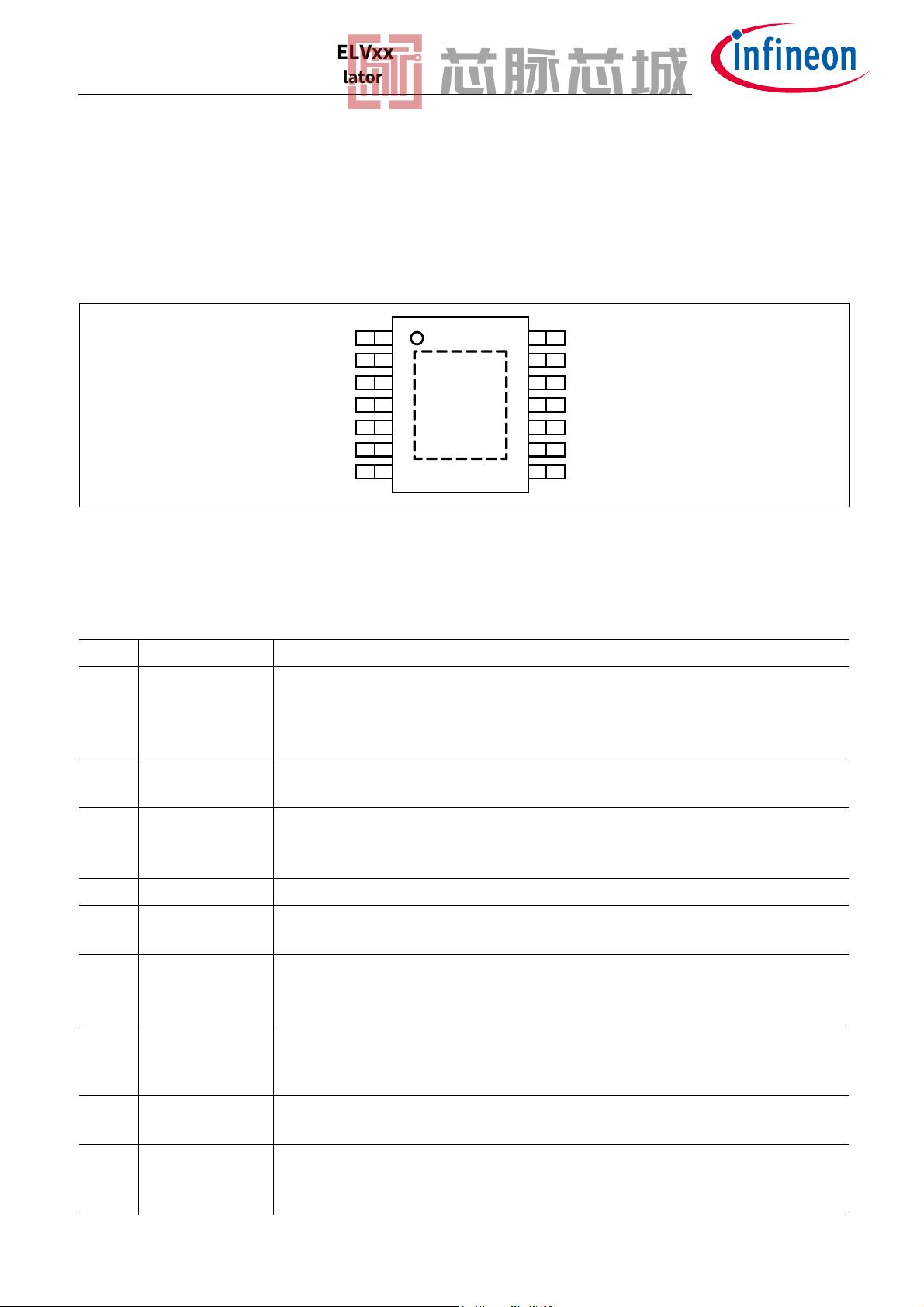
2 Pin configuration . . . . . . . . . . . . . . . . . . . . . . . . . . . . . . . . . . . . . . . . . . . . . . . . . . . . . . . . . . . . . . . . . 5
2.1 Pin assignment TLS820F0ELV50 and TLS820F0ELV33 . . . . . . . . . . . . . . . . . . . . . . . . . . . . . . . . . . . . . . . . . 5
2.2 Pin definitions and functions TLS820F0ELV50 and TLS820F0ELV33 . . . . . . . . . . . . . . . . . . . . . . . . . . . . 5
3 General product characteristics . . . . . . . . . . . . . . . . . . . . . . . . . . . . . . . . . . . . . . . . . . . . . . . . . . . . 7
3.1 Absolute maximum ratings . . . . . . . . . . . . . . . . . . . . . . . . . . . . . . . . . . . . . . . . . . . . . . . . . . . . . . . . . . . . . . . . 7
3.2 Functional range . . . . . . . . . . . . . . . . . . . . . . . . . . . . . . . . . . . . . . . . . . . . . . . . . . . . . . . . . . . . . . . . . . . . . . . . . 8
3.3 Thermal resistance . . . . . . . . . . . . . . . . . . . . . . . . . . . . . . . . . . . . . . . . . . . . . . . . . . . . . . . . . . . . . . . . . . . . . . . 9
4 Block description and electrical characteristics . . . . . . . . . . . . . . . . . . . . . . . . . . . . . . . . . . . . . . 10
4.1 Voltage regulation . . . . . . . . . . . . . . . . . . . . . . . . . . . . . . . . . . . . . . . . . . . . . . . . . . . . . . . . . . . . . . . . . . . . . . . 10
4.2 Typical performance characteristics voltage regulator . . . . . . . . . . . . . . . . . . . . . . . . . . . . . . . . . . . . . . 13
4.3 Current consumption . . . . . . . . . . . . . . . . . . . . . . . . . . . . . . . . . . . . . . . . . . . . . . . . . . . . . . . . . . . . . . . . . . . . 16
4.4 Typical performance characteristics current consumption . . . . . . . . . . . . . . . . . . . . . . . . . . . . . . . . . . . 17
4.5 Enable . . . . . . . . . . . . . . . . . . . . . . . . . . . . . . . . . . . . . . . . . . . . . . . . . . . . . . . . . . . . . . . . . . . . . . . . . . . . . . . . . . 18
4.6 Typical performance characteristics enable . . . . . . . . . . . . . . . . . . . . . . . . . . . . . . . . . . . . . . . . . . . . . . . . 19
4.7 Reset . . . . . . . . . . . . . . . . . . . . . . . . . . . . . . . . . . . . . . . . . . . . . . . . . . . . . . . . . . . . . . . . . . . . . . . . . . . . . . . . . . . 20
4.8 Typical performance characteristics reset . . . . . . . . . . . . . . . . . . . . . . . . . . . . . . . . . . . . . . . . . . . . . . . . . . 25
4.9 Standard watchdog . . . . . . . . . . . . . . . . . . . . . . . . . . . . . . . . . . . . . . . . . . . . . . . . . . . . . . . . . . . . . . . . . . . . . . 26
4.10 Typical performance characteristics standard watchdog . . . . . . . . . . . . . . . . . . . . . . . . . . . . . . . . . . . . 34
5 Application information . . . . . . . . . . . . . . . . . . . . . . . . . . . . . . . . . . . . . . . . . . . . . . . . . . . . . . . . . . 35
5.1 Application diagram . . . . . . . . . . . . . . . . . . . . . . . . . . . . . . . . . . . . . . . . . . . . . . . . . . . . . . . . . . . . . . . . . . . . . 35
5.2 Selection of external components . . . . . . . . . . . . . . . . . . . . . . . . . . . . . . . . . . . . . . . . . . . . . . . . . . . . . . . . . 35
5.2.1 Input pin . . . . . . . . . . . . . . . . . . . . . . . . . . . . . . . . . . . . . . . . . . . . . . . . . . . . . . . . . . . . . . . . . . . . . . . . . . . . . . 35
5.2.2 Output pin . . . . . . . . . . . . . . . . . . . . . . . . . . . . . . . . . . . . . . . . . . . . . . . . . . . . . . . . . . . . . . . . . . . . . . . . . . . . 35
5.3 Thermal considerations . . . . . . . . . . . . . . . . . . . . . . . . . . . . . . . . . . . . . . . . . . . . . . . . . . . . . . . . . . . . . . . . . . 36
5.4 Reverse polarity protection . . . . . . . . . . . . . . . . . . . . . . . . . . . . . . . . . . . . . . . . . . . . . . . . . . . . . . . . . . . . . . . 37
5.5 Further application information . . . . . . . . . . . . . . . . . . . . . . . . . . . . . . . . . . . . . . . . . . . . . . . . . . . . . . . . . . . 37
6 Package information . . . . . . . . . . . . . . . . . . . . . . . . . . . . . . . . . . . . . . . . . . . . . . . . . . . . . . . . . . . . . 38
7 Revision history . . . . . . . . . . . . . . . . . . . . . . . . . . . . . . . . . . . . . . . . . . . . . . . . . . . . . . . . . . . . . . . . . 39
Table of contents
![](https://csdnimg.cn/release/download_crawler_static/88026931/bg4.jpg)
Datasheet 4 Rev. 1.2
2021-04-08
OPTIREG™ linear TLS820F0ELVxx
Low dropout linear voltage regulator
Block diagram
1 Block diagram
Figure 1 Block diagram TLS820F0ELV50 and TLS820F0ELV33
Bandgap
Reference
GND
Q
I
Temperature
Shutdown
EN
Enable
Reset
RO
RADJ
DT1
Watchdog
WI
WO
DT2
Current
Limitation
![](https://csdnimg.cn/release/download_crawler_static/88026931/bg5.jpg)
Datasheet 5 Rev. 1.2
2021-04-08
OPTIREG™ linear TLS820F0ELVxx
Low dropout linear voltage regulator
Pin configuration
2 Pin configuration
2.1 Pin assignment TLS820F0ELV50 and TLS820F0ELV33
Figure 2 Pin configuration
2.2 Pin definitions and functions TLS820F0ELV50 and TLS820F0ELV33
Pin Symbol Function
1I Input
It is recommended to place a small ceramic capacitor (e.g. 100 nF) to GND, close
to the IC terminals, in order to compensate line influences. See also
Chapter 5.2.1
2, 4, 6 n.c. Not connected
Leave open or connect to GND
3EN Enable (integrated pull-down resistor)
Enable the IC with high level input signal;
Disable the IC with low level input signal;
5GND Ground
7WI Watchdog input (integrated pull-down resistor)
Serve Watchdog with trigger input signal (usable for microcontroller monitoring)
8RADJ Reset threshold adjustment
Connect to GND to use standard value;
Connect an external voltage divider to adjust reset threshold
9DT1 Delay timing 1 (integrated pull-down resistor)
Connect to GND or Q to select Reset timing acc. to Table 8
Connect to GND or Q to select Watchdog timing acc. to Table 11
10 DT2 Delay timing 2 (integrated pull-down resistor)
Connect to GND or Q to select Watchdog timing acc. to Table 11
11 RO Reset output (integrated pull-up resistor to Q)
Open collector output;
Leave open if the reset function is not needed
I
n.c.
n.c.
GND
Q
n.c.
WI
n.c.
WO
RO
DT1
DT2
RADJ
1
2
3
4
5
6
7
14
13
12
11
10
9
8
SSOP-14
EN
剩余39页未读,继续阅读
资源评论
![avatar-default](https://csdnimg.cn/release/downloadcmsfe/public/img/lazyLogo2.1882d7f4.png)
![avatar](https://profile-avatar.csdnimg.cn/default.jpg!1)
芯脉芯城
- 粉丝: 3
- 资源: 4031
上传资源 快速赚钱
我的内容管理 展开
我的资源 快来上传第一个资源
我的收益
登录查看自己的收益我的积分 登录查看自己的积分
我的C币 登录后查看C币余额
我的收藏
我的下载
下载帮助
![voice](https://csdnimg.cn/release/downloadcmsfe/public/img/voice.245cc511.png)
![center-task](https://csdnimg.cn/release/downloadcmsfe/public/img/center-task.c2eda91a.png)
安全验证
文档复制为VIP权益,开通VIP直接复制
![dialog-icon](https://csdnimg.cn/release/downloadcmsfe/public/img/green-success.6a4acb44.png)