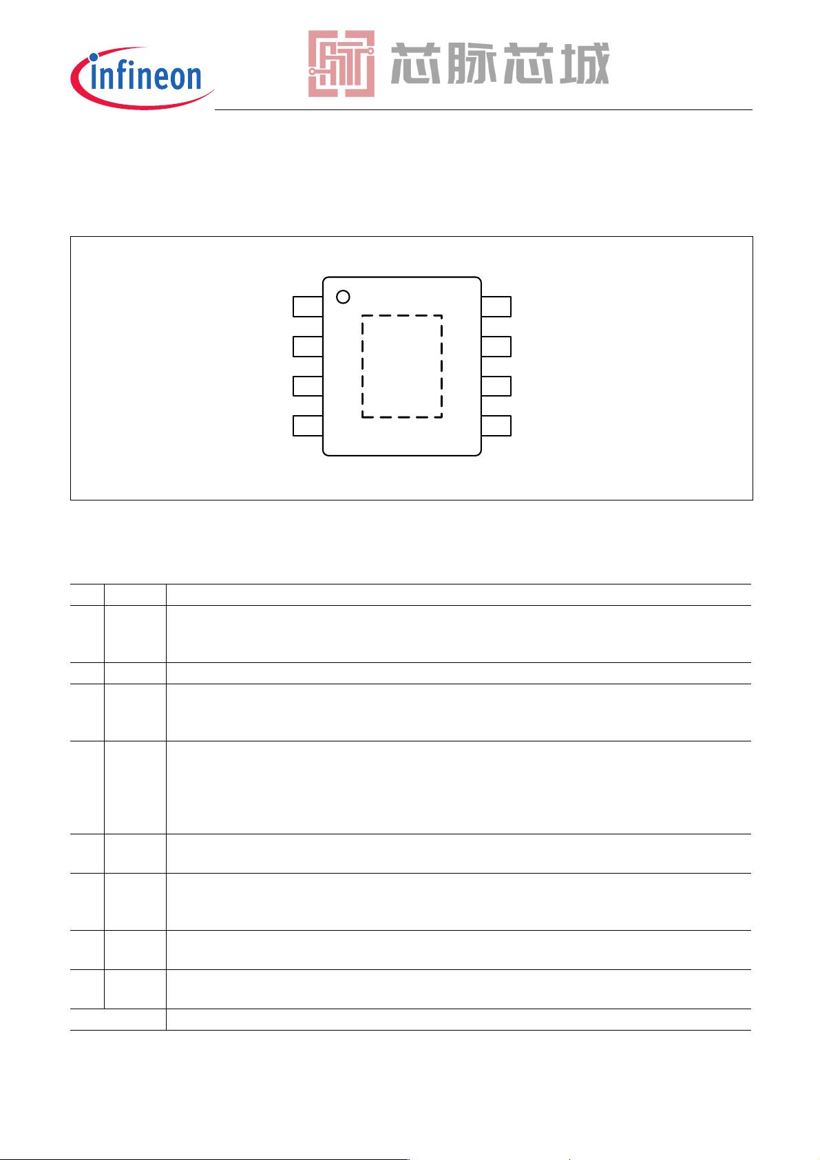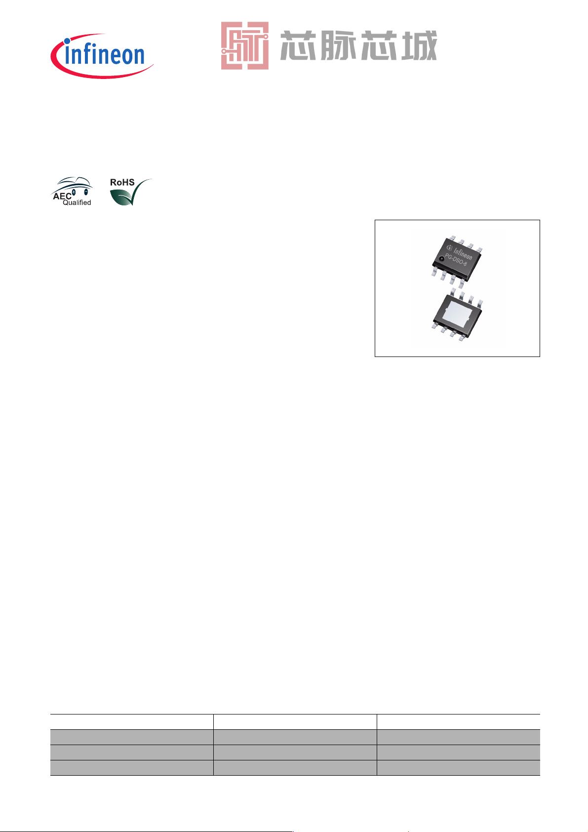
PG-DSO-8
Type Package Marking
TLE8366EV50 PG-DSO-8 8366EV50
TLE8366EV33 PG-DSO-8 8366EV33
TLE8366EV PG-DSO-8 8366EV
Data sheet 2 Rev. 1.0, 2009-05-18
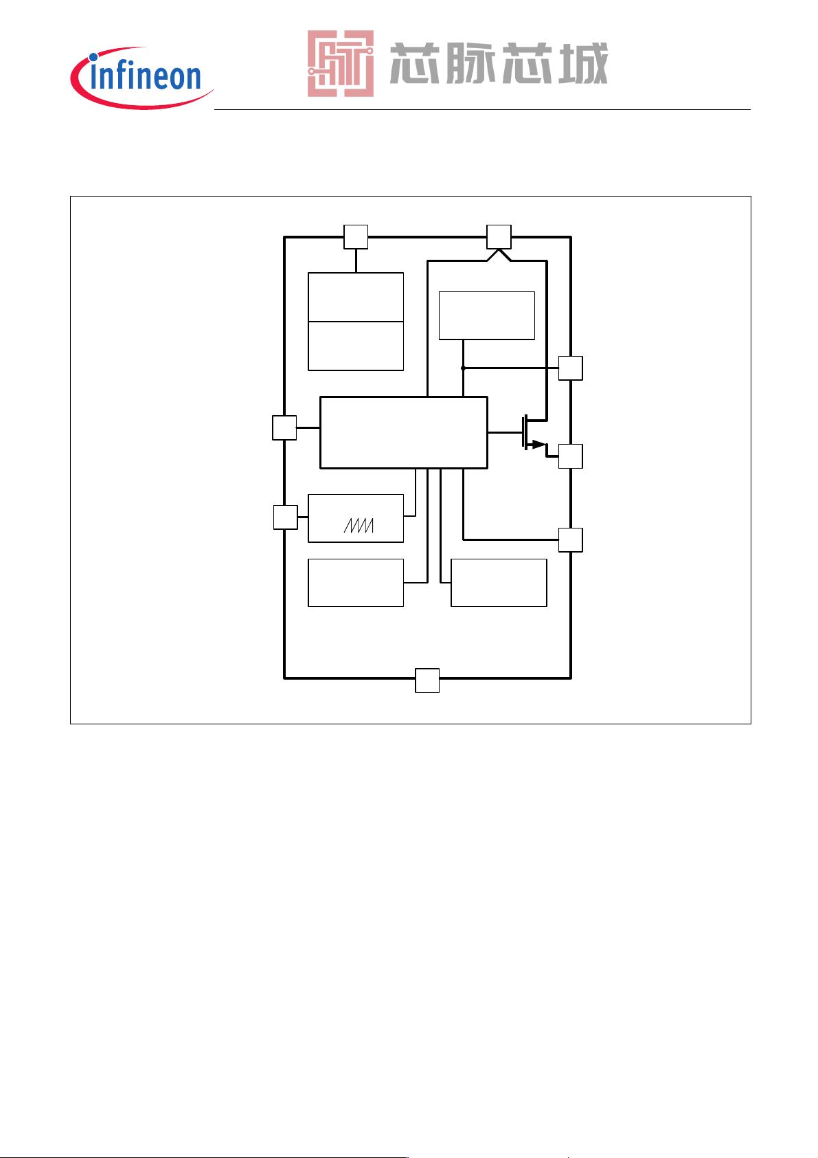
1.8A DC/DC Step-Down Voltage Regulator TLE8366
1Overview
• 1.8A step down voltage regulator
• Output voltage versions: 5.0 V, 3.3 V and adjustable
• ± 2% output voltage tolerance (+-4% for full load current range)
• Integrated power transistor
• PWM regulation with feedforward
• Input voltage range from 4.75V to 45V
• 370 kHz switching frequency
• Synchronization input
• Very low shutdown current consumption (<2uA)
• Soft-start function
• Input undervoltage lockout
• Suited for automotive applications:
T
j
= -40 °C to +150 °C
• Green Product (RoHS compliant)
• AEC Qualified
Description
The TLE8366 is a PWM step-down DC/DC converter with an integrated 1.8 A power switch, packaged in a small
PG-DSO-8 with exposed pad. There are three versions available, two fixed voltage with 5.0 V (TLE8366EV50) or
3.3 V (TLE8366EV33) and a variable voltage variant named TLE8366EV with a reference feedback voltage of only
600 mV. The wide input voltage range from 4.75 to 45 V makes the TLE8366 suitable for a wide variety of
applications. The device is designed to be used under harsh automotive environment.
The switching frequency of nominal 370 kHz allows the use of small and cost-effective inductors and capacitors,
resulting in a low, predictable output ripple and in minimized consumption of board space. (If desired the device
could be synchronized to an external frequency source between 200 and 530 kHz.)
The TLE8366 includes safety features such as a cycle-by-cycle current limitation, over-temperature shutdown and
input under voltage lockout. The enable function, in shutdown mode with less than 2 µA current consumption,
enables easy power management in battery-powered systems.
The voltage regulation loop provides an excellent line and load regulation. The stability of the loop could be
adjusted by using an external compensation network. This compensation network combined with voltage mode
regulation and a feed-forward control path guarantees a highly effective line transient rejection. During start-up the
integrated soft-start limits the inrush current peak and prevents from a voltage overshoot.