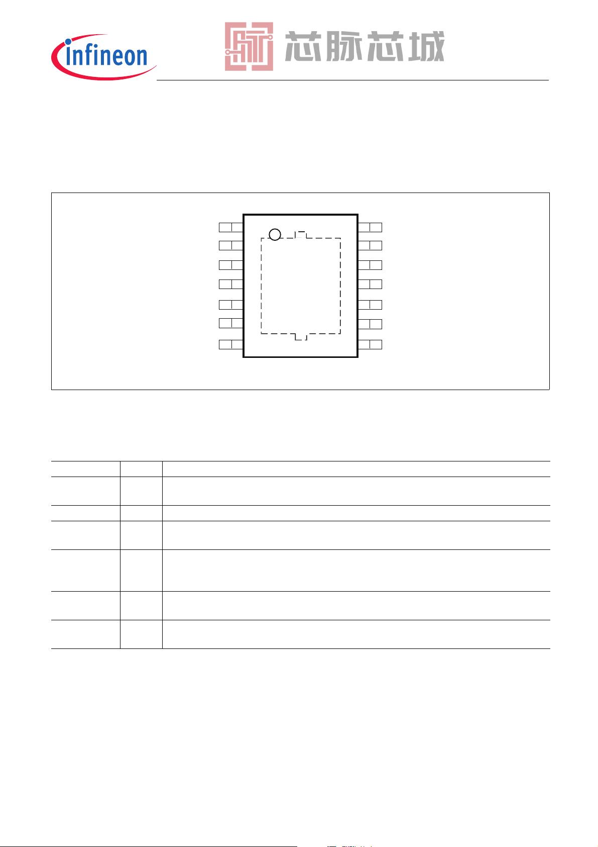
PG-SSOP-14 Exposed Pad
PG-TO252-3
PG-TO263-3
Type Package Marking
TLE7274-2E PG-SSOP-14 Exposed Pad 7274-2E
TLE7274-2D PG-TO252-3 7274-2D
TLE7274-2G PG-TO263-3 7274-2G
Data Sheet 2 Rev. 1.01, 2011-11-30
TLE7274-25-V Low Dropout Voltage Regulator
1Overview
Features
• Ultra Low Current Consumption 20 μA
• Output Voltage 5 V ±2%
• Output Current up to 300 mA
• Very Low Dropout Voltage
• Output Current Limitation
• Overtemperature Shutdown
• Wide Temperature Range From -40 °C up to 150 °C
• Green Product (RoHS compliant)
• AEC Qualified
Description
The TLE7274-2 is a monolithic integrated low dropout voltage regulator
for load currents up to 300 mA. An input voltage up to 42 V is regulated
to
V
Q,nom
= 5.0 V with a precision of ±2%. The sophisticated design allows
to achieve stable operation even with ceramic output capacitors down to
470 nF. The device is designed for the harsh environment of automotive
applications. Therefore it is protected against overload, short circuit and
overtemperature conditions by the implemented output current limitation
and the overtemperature shutdown circuit. The TLE7274-2 can be also
used in all other applications requiring a stabilized 5 V voltage.
Due to its ultra low quiescent current of typically 20 µA the TLE7274-2 is
dedicated for use in applications permanently connected to
V
BAT
. An
integrated output sink current circuitry keeps the voltage at the Output pin
Q below 5.5 V even in case of occuring reverse currents. Thus connected
devices are protected from overvoltage damage. For applications
requiring extremely low noise levels the Infineon voltage regulator family
TLE 42XX and TLE 44XX is more suited than the TLE7274-2. A mV-
range output noise on the TLE7274-2 caused by the charge pump
operation is unavoidable due to the ultra low quiescent current concept.